|
数据搜索系统,热门电子元器件搜索 |
|
|
数据搜索系统,热门电子元器件搜索 |
|
RC19302A00AGNT#KD0 数据表(PDF) 45 Page - Renesas Technology Corp |
|
|
|||||||||||||||||||||||||||||
RC19302A00AGNT#KD0 数据表(HTML) 45 Page - Renesas Technology Corp |
|
|
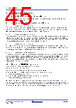
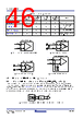
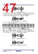
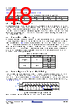
45 / 62 page  R31DS0210EU0106 Rev.1.06 Page 45 May 11, 2026 RC193xx Datasheet 5. Applications Information 5.1 Inputs, Outputs, and Output Enable Control The CLKIN/CLKINb inputs of the RC193xx devices have an internal bias network that prevents self-oscillation from a floating input clock condition. 5.1.1 Recommendations for Unused Inputs and Outputs 5.1.1.1 Unused Differential CLKIN Inputs The CLKIN/CLKINb inputs of the RC19xxx devices have internal bias networks that protect the devices from a floating input clock condition. For RC193xx multiplexers that use only one input clock, the unused input can be left open. Renesas recommends that no trace be attached to unused CLKIN pins. 5.1.1.2 Unused Single-ended Control Inputs The single-ended control pins have internal pull-up and/or internal pull-down resistors and do not require external resistors. They can be left floating if the default pin state is the desired state. If external resistors are needed to change the pin state or are desired for design robustness, 10kohm is the recommended value. Tri-level inputs are internally biased to VDD/2 and will indicate the mid (M) state if left floating. 5.1.1.3 Unused Differential CLK Outputs All unused CLK outputs can be left floating. Renesas recommends that no trace be attached to unused CLK outputs. While not required (but highly recommended), the best design practice is to disable unused CLK outputs. This is easily accomplished with the dedicated OEb pin for each output. 5.1.1.4 Unused SMBus Clock and Data Pins If the SMBus interface is not used, the clock and data pins must be pulled high with an external resistor. The two pins can share a resistor if there is no possibility of using the SMBus interface for debug purposes. If the interface might be used for debug, separate resistors should be used. Lightly loaded buses may use 10kohm pull-up resistors. Heavily loaded buses will require smaller pull-up resistor values. The SMBus pins are 3.3V tolerant and may be used with a 3.3V pull-up voltage 5.2 Differential CLKIN Configurations The RC193xx input clock buffer supports four configurations: ▪ Direct connection to HCSL-level inputs ▪ Direct connection to LVDS-level inputs with external termination resistor ▪ Internal self-bias circuit for applications that externally AC-couple the input clock This feature is enabled by the AC_IN bit. ▪ Internal pull-down resistors (Rp) to terminate the clock input at the receiver. This feature is enabled by the Rx_TERM bit. Devices with multiple input clocks have individual AC_IN and Rx_TERM configuration bits for each input. The internal input clock terminations prevent reflections and are useful for non-PCIe applications, where the frequency and transmission line length vary from the 100MHz PCIe standard. The following table summarizes the CLKIN configuration bit settings for the various configurations that are displayed in Figure 13 to Figure 16. |
|
链接网址 |
| ALLDATASHEET是否为您带来帮助? [ DONATE ] |
关于 Alldatasheet | 广告服务 | 联系我们 | 隐私政策 | 数据表链接 | 链接交换 | 制造商名单 All Rights Reserved©Alldatasheet.com |
| Russian : Alldatasheetru.com | Korean : Alldatasheet.co.kr | Spanish : Alldatasheet.es | French : Alldatasheet.fr | Italian : Alldatasheetit.com Portuguese : Alldatasheetpt.com | Polish : Alldatasheet.pl | Vietnamese : Alldatasheet.vn Indian : Alldatasheet.in | Mexican : Alldatasheet.com.mx | British : Alldatasheet.co.uk | New Zealand : Alldatasheet.co.nz |
|
Family Site : ic2ic.com |
icmetro.com |
 Chinese ▼
 English
 Chinese
 German
 Japanese
 Russian
 Korean
 Spanish
 French
 Italian
 Portuguese
 Polish
 Vietnamese
 Indian
 Mexican
 British
 New Zealand