|
数据搜索系统,热门电子元器件搜索 |
|
|
数据搜索系统,热门电子元器件搜索 |
|
RC19302A00AGNT#KD0 数据表(PDF) 19 Page - Renesas Technology Corp |
|
|
|||||||||||||||||||||||||||||
RC19302A00AGNT#KD0 数据表(HTML) 19 Page - Renesas Technology Corp |
|
|
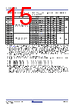
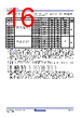
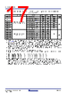
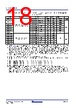
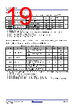
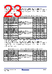
19 / 62 page  R31DS0210EU0106 Rev.1.06 Page 19 May 11, 2026 RC193xx Datasheet 2.4.2 Other Phase Jitter Note: Dual-mode operation (CLKSEL_tri = M, both CLKIN running) is recommended only for PCIe applications. 2.4.3 Output Frequencies, Startup Time, and LOS Timing Table 13. Non-PCIe Refclk Phase Jitter (CLKSEL_tri = 0 or 1, Unselected CLKIN Off) [1][2][3] 1. See Test Loads for test configuration. Measured with one input at 100MHz and the other at 156.25MHz. 2. SMA100B used as signal source. 3. RC19xxx devices meet all legacy QPI/UPI specifications by meeting the PCIe and DB2000Q specifications listed in this document. Symbol Parameter Conditions Typical Maximum Specification Limit Unit tjphDB2000Q Additive Phase Jitter - Normal conditions [4] 4. Differential input swing = 1600mV and input slew rate = 3.5V/ns. 100MHz, Intel-supplied filter [3] 11.5 12.8 80 [5] 5. The rms sum of the source jitter and the additive jitter must be less than the jitter specification listed. fs RMS tjph12k-20M 156.25MHz (12kHz to 20MHz) 42.8 45.7 N/A tjphDB2000Q Additive Phase Jitter - Degraded conditions [6] 6. Differential input swing = 800mV and input slew rate = 1.5V/ns. 100MHz, Intel-supplied filter [3] 11.5 13.7 80 [5] tjph12k-20M 156.25MHz (12kHz to 20MHz) 42.8 52.5 N/A Table 14. Output Frequencies, Startup Time, and LOS Timing Symbol Parameter Conditions Minimum Typical Maximum Unit fOP Operating Frequency Automatic Clock Parking (ACP) Circuit disabled. 1 - 400 MHz Automatic Clock Parking (ACP) Circuit enabled. 25 - 400 tSTARTUP Start-up Time [1] 1. Measured from when all power supplies have reached > 90% of nominal voltage to the first stable clock edge on the output. PWRGD_PGWRDNb tied to VDD in this case. - 0.5 1.6 ms [2] 2. VDD stable, measured from de-assertion of PWRGD_PWRDNb. - 70 85 ns tLATOEb OEb Latency OEb assertion/de-assertion CLK start/stop latency. Selected input clock must be running. 4 5 6 clks tLOSAssert LOS Assert Time Time from disappearance of selected input clock to LOS assert. [3][4] 3. The clock detect circuit does not qualify the accuracy of the input clock. 4. PWRGD_PWRDNb high. The clock detect circuit will park the outputs in a low/low state within this time. - 244 289 ns tLOSDeassert LOS De-assert Time Time from appearance of selected input clock to LOS de-assert. [2][5] 5. PWRGD_PWRDNb high. The clock detect circuit will drive the outputs to a high/low state within this time and then begin clocking the outputs. 6 - 7 clks |
|
链接网址 |
| ALLDATASHEET是否为您带来帮助? [ DONATE ] |
关于 Alldatasheet | 广告服务 | 联系我们 | 隐私政策 | 数据表链接 | 链接交换 | 制造商名单 All Rights Reserved©Alldatasheet.com |
| Russian : Alldatasheetru.com | Korean : Alldatasheet.co.kr | Spanish : Alldatasheet.es | French : Alldatasheet.fr | Italian : Alldatasheetit.com Portuguese : Alldatasheetpt.com | Polish : Alldatasheet.pl | Vietnamese : Alldatasheet.vn Indian : Alldatasheet.in | Mexican : Alldatasheet.com.mx | British : Alldatasheet.co.uk | New Zealand : Alldatasheet.co.nz |
|
Family Site : ic2ic.com |
icmetro.com |
 Chinese ▼
 English
 Chinese
 German
 Japanese
 Russian
 Korean
 Spanish
 French
 Italian
 Portuguese
 Polish
 Vietnamese
 Indian
 Mexican
 British
 New Zealand