|
数据搜索系统,热门电子元器件搜索 |
|
|
数据搜索系统,热门电子元器件搜索 |
|
EM357-RTR 数据表(PDF) 223 Page - List of Unclassifed Manufacturers |
|
|
|||||||||||||||||||||||||||||
EM357-RTR 数据表(HTML) 223 Page - List of Unclassifed Manufacturers |
|
|
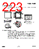
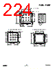
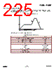
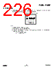
223 / 240 page  EM351 / EM357 19 Mechanical Details The EM35x package is a plastic 48-pin QFN that is 7 mm x 7 mm x 0.90 mm. Figure 19-1 illustrates the package drawing. Figure 19-1. Package Drawing 19.1 QFN48 Footprint Recommendations Figure 19-2 demonstrates the IPC-7351 recommended PCB Footprint for the EM35x (QFN50P700X700X90-49N). A ground pad in the bottom center of the package forms a 49th pin. A 3 x 3 array of non-thermal vias should connect the EM35x decal center shown in Figure 19-2 to the PCB ground plane through the ground pad. In order to properly solder the EM35x to the footprint, the Paste Mask layer should have a 3 x 3 array of circular openings at 1.015 mm diameter spaced approximately 1.625 mm (center to center) apart, as shown in Figure 19-3. This will cause an evenly distributed solder flow and coplanar attachment to the PCB. The solder mask layer (illustrated in Figure 19-4) should be the same as the copper layer for the EM35x footprint. For more information on the package footprint, please refer to the appropriate EM35x Reference Design. 19-1 120-035X-000D Preliminary |
|
链接网址 |
| ALLDATASHEET是否为您带来帮助? [ DONATE ] |
关于 Alldatasheet | 广告服务 | 联系我们 | 隐私政策 | 数据表链接 | 链接交换 | 制造商名单 All Rights Reserved©Alldatasheet.com |
| Russian : Alldatasheetru.com | Korean : Alldatasheet.co.kr | Spanish : Alldatasheet.es | French : Alldatasheet.fr | Italian : Alldatasheetit.com Portuguese : Alldatasheetpt.com | Polish : Alldatasheet.pl | Vietnamese : Alldatasheet.vn Indian : Alldatasheet.in | Mexican : Alldatasheet.com.mx | British : Alldatasheet.co.uk | New Zealand : Alldatasheet.co.nz |
|
Family Site : ic2ic.com |
icmetro.com |
 Chinese ▼
 English
 Chinese
 German
 Japanese
 Russian
 Korean
 Spanish
 French
 Italian
 Portuguese
 Polish
 Vietnamese
 Indian
 Mexican
 British
 New Zealand