|
数据搜索系统,热门电子元器件搜索 |
|
|
数据搜索系统,热门电子元器件搜索 |
|
EM357-RTR 数据表(PDF) 52 Page - List of Unclassifed Manufacturers |
|
|
|||||||||||||||||||||||||||||
EM357-RTR 数据表(HTML) 52 Page - List of Unclassifed Manufacturers |
|
|
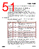
52 / 240 page  EM351 / EM357 Table 7-2. Timer 2 Output Configuration Controls GPIO Mapping Selected by TIM2_OR Bit Timer 2 Output Option Register Bit 0 1 TIM2C1 TIM2_OR[4] PA0 PB1 TIM2C2 TIM2_OR[5] PA3 PB2 TIM2C3 TIM2_OR[6] PA1 PB3 TIM2C4 TIM2_OR[7] PA2 PB4 For outputs assigned to the serial controllers, the serial interface mode registers (SCx_MODE) determine how the GPIO pins are used. The alternate outputs of PA4 and PA5 can either provide packet trace data (PTI_EN and PTI_DATA), or synchronous CPU trace data (TRACEDATA2 and TRACEDATA3). The selection of packet trace or CPU trace is made through the Ember software. If a GPIO does not have an associated peripheral in alternate output mode, its output is set to 0. 7.3 Forced Functions For some GPIOs the GPIO_PxCFGH/L configuration will be overridden. These functions are forced when the EM35x is reset and remain forced until software overrides the forced functions. Table 7-3 shows the GPIOs that have different functions forced on them regardless of the GPIO_PxCFGH/L registers. Table 7-3. GPIO Forced Functions GPIO Forced Mode Forced Signal PA7 Open-drain output REG_EN PC0 Input with pull up JRST PC2 Push-pull output JTDO PC3 Input with pull up JDTI PC41 Input with pull up JTMS PC41 Bidirectional (push-pull output or floating input) controlled by debugger interface SWDIO 1 The choice of PC4’s forced signal is controlled by an external debug tool. JTMS is forced when the SWJ is in JTAG mode and SWDIO is forced when the SWJ is in Serial Wire mode. PA7 is forced to be the regulator enable signal, REG_EN. If an external regulator is used and controlled through REG_EN, PA7’s forced functionality must not be overridden. If an external regulator is not used, REG_EN may be disabled and PA7 may be reclaimed as a normal GPIO. Disabling REG_EN is done by clearing the bit GPIO_EXTREGEN in the GPIO_DBGCFG register. PC0, PC2, PC3, and PC4 are forced to be the Serial Wire and JTAG (SWJ) Interface. When the EM35x resets, these four GPIOs are forced to operate in JTAG mode. Switching the debug interface between JTAG mode and Serial Wire mode can only be accomplished by the external debug tool and cannot be affected by software executing on the EM35x. Due to the fact that Serial Wire mode can only be invoked by an external debug tool 7-3 120-035X-000D Preliminary |
|
链接网址 |
| ALLDATASHEET是否为您带来帮助? [ DONATE ] |
关于 Alldatasheet | 广告服务 | 联系我们 | 隐私政策 | 数据表链接 | 链接交换 | 制造商名单 All Rights Reserved©Alldatasheet.com |
| Russian : Alldatasheetru.com | Korean : Alldatasheet.co.kr | Spanish : Alldatasheet.es | French : Alldatasheet.fr | Italian : Alldatasheetit.com Portuguese : Alldatasheetpt.com | Polish : Alldatasheet.pl | Vietnamese : Alldatasheet.vn Indian : Alldatasheet.in | Mexican : Alldatasheet.com.mx | British : Alldatasheet.co.uk | New Zealand : Alldatasheet.co.nz |
|
Family Site : ic2ic.com |
icmetro.com |
 Chinese ▼
 English
 Chinese
 German
 Japanese
 Russian
 Korean
 Spanish
 French
 Italian
 Portuguese
 Polish
 Vietnamese
 Indian
 Mexican
 British
 New Zealand