|
数据搜索系统,热门电子元器件搜索 |
|
|
数据搜索系统,热门电子元器件搜索 |
|
AD9739-R2-EBZ 数据表(PDF) 38 Page - Analog Devices |
|
|
|||||||||||||||||||||||||||||
AD9739-R2-EBZ 数据表(HTML) 38 Page - Analog Devices |
|
|
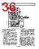
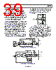
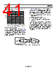
38 / 48 page  AD9739 Data Sheet Rev. B | Page 38 of 48 ANALOG INTERFACE CONSIDERATIONS ANALOG MODES OF OPERATION The AD9739 uses the quad-switch architecture shown in Figure 54. The quad-switch architecture masks the code-dependent glitches that occur in a conventional two-switch DAC. Figure 55 compares the waveforms for a conventional DAC and the quad-switch DAC. In the two-switch architecture, a code-dependent glitch occurs each time the DAC switches to a different state (that is, D1 to D2). This code-dependent glitching causes an increased amount of distortion in the DAC. In a quad-switch architecture (no matter what the codes are), there are always two switches transitioning at each half clock cycle, thus eliminating the code- dependent glitches. However, a constant glitch occurs at 2 × DACCLK because half of the internal switches change state on the rising DACCLK edge, while the other half change state on the falling DACCLK edge. VG1 VDD IOUTP IOUTN VG1 G4 VG3 VG2 DACCLK_x CLK LATCHES DBx[13:0] VG2 VG3 VG4 V Figure 54. AD9739 Quad-Switch Architecture INPUT DATA DACCLK_x TWO-SWITCH DAC OUTPUT FOUR-SWITCH DAC OUTPUT (NORMAL MODE) t D1 D2 D3 D4 D5 D6 D7 D8 D9 D10 D6 D7 D8 D9 D10 D1 D2 D3 D4 D5 D6 D7 D8 D9 D10 D1 D2 D3 D4 D5 t Figure 55. Two-Switch and Quad-Switch DAC Waveforms Another attribute of the quad-switch architecture is that it also enables the DAC core to operate in one of the following three modes: normal mode, mix mode, and return-to-zero (RZ) mode. The mode is selected via SPI Register 0x08, Bits[1:0] with normal mode being the default value. In the mix mode, the output is effectively chopped at the DAC sample rate. This has the effect of reducing the power of the fundamental signal while increasing the power of the images centered around the DAC sample rate, thus improving the output power of these images. The RZ mode is similar to the analog mix mode, except that the intermediate data samples are replaced with midscale values. INPUT DATA DACCLK_x FOUR-SWITCH DAC OUTPUT ( fS MIX MODE) FOUR-SWITCH DAC OUTPUT (RETURN TO ZERO MODE) D6 D7 D8 D9 D10 D1 D2 D3 D4 D5 –D6 –D7 –D8 –D9 –D10 D6 D7 D8 D9 D10 –D1 –D2 –D3 –D4 –D5 D1 D2 D3 D4 D5 D6 D7 D8 D9 D10 D1 D2 D3 D4 D5 t t Figure 56. Mix-Mode and RZ DAC Waveforms Figure 56 shows the DAC waveforms for both the mix mode and the RZ mode. Note that the disadvantage of the RZ mode is the 6 dB loss of power to the load because the DAC is only functioning for ½ the DAC update period. This ability to change modes provides the user the flexibility to place a carrier anywhere in the first three Nyquist zones, depending on the operating mode selected. Switching between the analog modes reshapes the sinc roll-off inherent at the DAC output. The maximum amplitude in all three Nyquist zones is impacted by this sinc roll-off, depending on where the carrier is placed (see Figure 57). As a practical matter, the usable bandwidth in the third Nyquist zone becomes limited at higher DAC clock rates (that is, >2 GSPS) when the output bandwidth of DAC core and the interface network (that is, balun) contributes to additional roll-off. FREQUENCY (Hz) 0FS 1.50FS 1.25FS 1.00FS 0.75FS 0.50FS 0.25FS –35 –30 –25 –20 –15 –10 –5 0 FIRST NYQUIST ZONE SECOND NYQUIST ZONE THIRD NYQUIST ZONE MIX MODE RZ MODE NORMAL MODE Figure 57. Sinc Roll-Off for Each Analog Operating Mode |
|
链接网址 |
| ALLDATASHEET是否为您带来帮助? [ DONATE ] |
关于 Alldatasheet | 广告服务 | 联系我们 | 隐私政策 | 数据表链接 | 链接交换 | 制造商名单 All Rights Reserved©Alldatasheet.com |
| Russian : Alldatasheetru.com | Korean : Alldatasheet.co.kr | Spanish : Alldatasheet.es | French : Alldatasheet.fr | Italian : Alldatasheetit.com Portuguese : Alldatasheetpt.com | Polish : Alldatasheet.pl | Vietnamese : Alldatasheet.vn Indian : Alldatasheet.in | Mexican : Alldatasheet.com.mx | British : Alldatasheet.co.uk | New Zealand : Alldatasheet.co.nz |
|
Family Site : ic2ic.com |
icmetro.com |
 Chinese ▼
 English
 Chinese
 German
 Japanese
 Russian
 Korean
 Spanish
 French
 Italian
 Portuguese
 Polish
 Vietnamese
 Indian
 Mexican
 British
 New Zealand