|
数据搜索系统,热门电子元器件搜索 |
|
|
数据搜索系统,热门电子元器件搜索 |
|
AD9739-R2-EBZ 数据表(PDF) 44 Page - Analog Devices |
|
|
|||||||||||||||||||||||||||||
AD9739-R2-EBZ 数据表(HTML) 44 Page - Analog Devices |
|
|
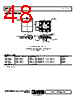
44 / 48 page  AD9739 Data Sheet Rev. B | Page 44 of 48 LAB EVALUATION OF THE AD9739 Figure 72 shows a recommended lab setup that was used to characterize the performance of the AD9739. The DPG2 is a dual port LVDS/CMOS data pattern generator available from Analog Devices, Inc., with an up to 1.25 GSPS data rate. The DPG2 directly interfaces to the AD9739 evaluation board via Tyco Z-PACK HM-Zd connectors. A low phase noise/jitter RF source, such as an R&S SMA100A signal generator, is used for the DAC clock. A 5 V power supply is used to power up the AD9739 evaluation board, and SMA cabling is used to interface to the supply, clock source, and spectrum analyzer. A USB 2.0 interface to a host PC is used to communicate to both the AD9739 evaluation board and the DPG2. A high dynamic range spectrum analyzer is required to evaluate the AD9739 reconstructed waveform’s ac performance. This is especially the case when measuring ACLR performance for high dynamic range applications, such as multicarrier DOCSIS CMTS applications. Harmonic, SFDR, and IMD measurements pertaining to unmodulated carriers can benefit by using a sufficiently high RF attenuation setting because these artifacts are easy to identify above the spectrum analyzer noise floor. However, reconstructed waveforms having modulated carrier(s) often benefit from the use of a high dynamic range RF amplifier and/or passive filters to measure close-in and wideband ACLR performance when using spectrum analyzers of limited dynamic range. ADI PATTERN GENERATOR DPG2 AD9739 EVAL. BOARD RHODE AND SCHWARTZ SMA 100A AGILENT PSA E4440A 10 MHz REFIN 10 MHz REOUT LAB PC USB 2.0 GPIB LVDS DATA AND DCI DCO 1.6GHz TO 2.5GHz 3dBm POWER SUPPLY +5V Figure 72. Lab Test Setup Used to Characterize the AD9739 POWER DISSIPATION AND SUPPLY DOMAINS The power dissipation of the AD9739 is dependent on the DAC clock rate as shown in Figure 73 and Figure 74. The current consumption from the 3.3 V supply remains relatively constant because it is used for biasing the DAC core (that is, VDDA) and differential input receivers (that is, VDD33). However, the current consumption from the 1.8 V supply is clock rate dependent and increases linearly with frequency because this supply is used by the digital path (that is, VDD) as well as the clock distribution circuitry (that is, VDDC). Treat the VDDC supply as an analog supply because the clock distribution circuitry has poor power supply rejection; therefore, noise on this supply can induce clock jitter. To ensure low noise on this sensitive supply, use a separate 1.8 V regulator powered from the 3.3 V analog supply rail that is also used to power VDDA. This supply rail can also be used to power-up VDD33 via an LC filter network. The digital 1.8 V supply, VDD, can be supplied via a well-filtered switching regulator. 0 0.1 0.2 0.3 0.4 0.5 0.6 0.7 0.8 0.9 1.0 1.1 1.2 0 250 500 750 1000 1250 1500 1750 2000 2250 2500 TOTAL VDD VDDC VDDA VDD33 fDAC (MHz) Figure 73. Power Consumption vs. fDAC @ 25°C 0 30 60 90 120 150 180 210 240 270 300 330 360 0 250 500 750 1000 1250 1500 1750 2000 2250 2500 I_VDD I_VDDC I_VDDA fDAC (MHz) I_VDD33 Figure 74. Current Consumption vs. fDAC @ 25°C |
|
链接网址 |
| ALLDATASHEET是否为您带来帮助? [ DONATE ] |
关于 Alldatasheet | 广告服务 | 联系我们 | 隐私政策 | 数据表链接 | 链接交换 | 制造商名单 All Rights Reserved©Alldatasheet.com |
| Russian : Alldatasheetru.com | Korean : Alldatasheet.co.kr | Spanish : Alldatasheet.es | French : Alldatasheet.fr | Italian : Alldatasheetit.com Portuguese : Alldatasheetpt.com | Polish : Alldatasheet.pl | Vietnamese : Alldatasheet.vn Indian : Alldatasheet.in | Mexican : Alldatasheet.com.mx | British : Alldatasheet.co.uk | New Zealand : Alldatasheet.co.nz |
|
Family Site : ic2ic.com |
icmetro.com |
 Chinese ▼
 English
 Chinese
 German
 Japanese
 Russian
 Korean
 Spanish
 French
 Italian
 Portuguese
 Polish
 Vietnamese
 Indian
 Mexican
 British
 New Zealand