|
数据搜索系统,热门电子元器件搜索 |
|
|
数据搜索系统,热门电子元器件搜索 |
|
AD9739-R2-EBZ 数据表(PDF) 39 Page - Analog Devices |
|
|
|||||||||||||||||||||||||||||
AD9739-R2-EBZ 数据表(HTML) 39 Page - Analog Devices |
|
|
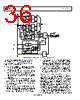
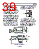
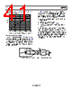
39 / 48 page  Data Sheet AD9739 Rev. B | Page 39 of 48 CLOCK INPUT CONSIDERATIONS The quality of the clock source and its drive strength are important considerations in maintaining the specified ac performance. The phase noise and spur characteristics of the clock source should be selected to meet the target application requirements. Phase noise and spurs at a given frequency offset on the clock source are directly translated to the output signal. It can be shown that the phase noise characteristics of a reconstructed output sine wave are related to the clock source by 20 × log10 (fOUT/fCLK) when the DAC clock path contribution, along with thermal and quantization effects, are negligible. The AD9739 clock receiver provides optimum jitter performance when driven by a fast slew rate originating from the LVPECL or CML output drivers. For a low jitter sinusoidal clock source, the ADCLK914 can be used to square-up the signal and provide a CML input signal for the AD9739 clock receiver. Note that all specifications and characterization presented in the data sheet are with the ADCLK914 driven by a high quality RF signal generator with the clock receiver biased at a 800 mV level. A dc blocking capacitor is used between the clock driver output and clock receiver input to allow for different dc bias levels. To minimize signal loss for high clock rates, a high quality, dc blocking RF capacitor is recommended. Figure 60 shows a clock source based on the ADF4350 low phase noise/jitter PLL. The ADF4350 can provide output frequencies from 140 MHz up to 4.4 GHz with jitter as low as 0.5 ps rms. Each single-ended output can provide a squared-up output level that can be varied from −4 dBm to +5 dBm allowing for >2 V p-p output differential swings. The ADF4350 also includes an additional CML buffer that can be used to drive another AD9739 device. ESD DACCLK_P DACCLK_N VDDC VSSC CLKx_OFFSET DIR_x = 0 CLKx_OFFSET DIR_x = 0 4-BIT PMOS IOUT ARRAY 4-BIT NMOS IOUT ARRAY Figure 58. Clock Input and Common-Mode Control The AD9739 clock receiver features the ability to independently adjust the common-mode level of its inputs over a span of ±100 mV centered about its midsupply point (that is, VDDC/2) as well as an offset for hysteresis purposes. Figure 58 shows the equivalent input circuit of one of the inputs. ESD diodes are not shown for clarity purposes. It has been found through characterization that the optimum setting is for both inputs to be biased at approximately 0.8 V. This can be achieved by writing a 0x0F (corresponding to a −15) setting to both cross controller registers (that is, Register 0x22 and Register 0x23). D D Q VCC VEE VT Q VREF 50Ω 50Ω 50Ω 50Ω 50Ω DACCLK_P DACCLK_N 100Ω 1nF 1nF ADCLK914 AD9739 10nF 10nF 50Ω Figure 59. ADCLK914 Interface to the AD9739 CLK Input VCO PLL ADF4350 FREF 1.8V p-p VVCO 1nF 1nF AD9739 3.9nH RFOUTA– RFOUTA+ RFOUTA– RFOUTA+ 100Ω DACCLK_P DACCLK_N DIV-BY-2N N = 0 – 4 Figure 60. ADF4350 Interface to the AD9739 CLK Input |
|
链接网址 |
| ALLDATASHEET是否为您带来帮助? [ DONATE ] |
关于 Alldatasheet | 广告服务 | 联系我们 | 隐私政策 | 数据表链接 | 链接交换 | 制造商名单 All Rights Reserved©Alldatasheet.com |
| Russian : Alldatasheetru.com | Korean : Alldatasheet.co.kr | Spanish : Alldatasheet.es | French : Alldatasheet.fr | Italian : Alldatasheetit.com Portuguese : Alldatasheetpt.com | Polish : Alldatasheet.pl | Vietnamese : Alldatasheet.vn Indian : Alldatasheet.in | Mexican : Alldatasheet.com.mx | British : Alldatasheet.co.uk | New Zealand : Alldatasheet.co.nz |
|
Family Site : ic2ic.com |
icmetro.com |
 Chinese ▼
 English
 Chinese
 German
 Japanese
 Russian
 Korean
 Spanish
 French
 Italian
 Portuguese
 Polish
 Vietnamese
 Indian
 Mexican
 British
 New Zealand