|
数据搜索系统,热门电子元器件搜索 |
|
|
数据搜索系统,热门电子元器件搜索 |
|
NET2890 数据表(PDF) 15 Page - List of Unclassifed Manufacturers |
|
|
|||||||||||||||||||||||||||||
NET2890 数据表(HTML) 15 Page - List of Unclassifed Manufacturers |
|
|
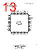
15 / 73 page  Specification NET2890 USB Interface Controller ____________________________________________________________________________________ NetChip Technology, Inc., 1999 335 Pioneer Way, Mountain View, California 94041 TEL (650) 526-1490 FAX (650) 526-1494 http://www.netchip.com Rev 2.0, Draft 9, July 16, 1999 15 IOW# 18 I, PU I/O Write. The I/O write strobe is asserted along with CS# and A[4:0] when a device on the local bus writes to an internal register or FIFO. It also allows a FIFO to be written during DMA transfers when DACK# is asserted. DRQ 19 O, 12mA, TP DMA Request. This signal indicates to an external DMA controller that a byte should be transferred to/from the FIFO. During a transfer, DRQ remains asserted until the DACK# input goes active. This output floats when the device is suspended by the USB Host. DACK# 20 I, PU DMA Acknowledge. This signal from an external DMA controller is used to transfer data to/from the FIFO in response to DRQ. IOR# and IOW# determine the direction of the DMA transfer. EOT# 21 I, PU End of Transfer. This signal from an external DMA controller is used to terminate a DMA transfer. If it is asserted during a DMA cycle, the current byte will be transferred, but no additional bytes will be requested. EOT# can be programmed to cause a USB interrupt. IRQ# 26 O, 12mA, OD Interrupt Request Output. The interrupt request output is used to interrupt a processor on the local bus. There are several sources of this interrupt which are described in the Register Description Section. USBOE# 27 I/O, 12mA, S, TS, PU USB Port Output Enable. When RESET# is not asserted, this is an active low output that is asserted when the NET2890 is driving the USB port data lines. It is intended for debugging purposes only. This signal is not driven while the device is suspended, but will be pulled high by the internal pull-up resistor. When RESET# is asserted, this pin is an input. Driving a LOW level during RESET# holds the NET2890 in a low-power mode by disabling the internal oscillator. DEVCFG# 28 O, 12mA, TP, PD Device Configured. This active low output is true when the NET2890 has been configured by the USB host. This bit is initialized to inactive (high) during reset and is controlled by the local CPU through the MAINCTL configuration register. This signal is not driven while the device is suspended, but will be pulled low by the internal pull-down resistor. If DEVCFG# is not needed locally, this signal can be used as a general output pin. SUSP# 33 O, 12mA, TP, PD Device Suspended. This active low output is true when the NET2890 has been suspended by the USB host. This signal is not driven while the device is suspended, but will be pulled low by the internal pull- down resistor. LCLK 16 O, 12mA, TP, PD Local Clock. This pin is a buffered clock output from either the internal 48 MHz oscillator or the derived USB clock, depending on the state of the “Local Clock Output” bits in the LOCALCTL configuration register. This signal is not driven while the device is suspended, but will be pulled low by the internal pull-down resistor. When the internal oscillator is started, LCLK is prevented from being driven for 2 msec. |
|
链接网址 |
| ALLDATASHEET是否为您带来帮助? [ DONATE ] |
关于 Alldatasheet | 广告服务 | 联系我们 | 隐私政策 | 数据表链接 | 链接交换 | 制造商名单 All Rights Reserved©Alldatasheet.com |
| Russian : Alldatasheetru.com | Korean : Alldatasheet.co.kr | Spanish : Alldatasheet.es | French : Alldatasheet.fr | Italian : Alldatasheetit.com Portuguese : Alldatasheetpt.com | Polish : Alldatasheet.pl | Vietnamese : Alldatasheet.vn Indian : Alldatasheet.in | Mexican : Alldatasheet.com.mx | British : Alldatasheet.co.uk | New Zealand : Alldatasheet.co.nz |
|
Family Site : ic2ic.com |
icmetro.com |
 Chinese ▼
 English
 Chinese
 German
 Japanese
 Russian
 Korean
 Spanish
 French
 Italian
 Portuguese
 Polish
 Vietnamese
 Indian
 Mexican
 British
 New Zealand