|
数据搜索系统,热门电子元器件搜索 |
|
|
数据搜索系统,热门电子元器件搜索 |
|
AD4052BCPZ-R2 数据表(PDF) 7 Page - Analog Devices |
|
|
|||||||||||||||||||||||||||||
AD4052BCPZ-R2 数据表(HTML) 7 Page - Analog Devices |
|
|
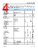
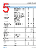
7 / 66 page  Data Sheet AD4052/AD4058 SPECIFICATIONS analog.com Rev. B | 7 of 66 TIMING SPECIFICATIONS VDD = VREF = 2.3 V to 3.6 V, VIO = 1.71 V to 3.6 V, digital output load capacitance (CLOAD) = 20 pF, and all other features in default configuration. Minimum and maximum limits at TA = −40°C to +125°C and typical values at TA = +25°C, unless otherwise indicated. Table 2. ADC Timing Specifications Parameter1 Symbol Min Typ Max Unit Sampling Rate2 fS AD4052 2 MSPS AD4058 500 kSPS Sample Period (Time Between Conversions)2 tCYC AD4052 500 ns AD4058 2000 ns Conversion Time tCONV 270 320 ns Acquisition Time3, 4 tACQ fS = 2 MSPS 290 327 ns fS = 500 kSPS 1790 1827 ns Quiet Time (Last SCLK Edge to CNV Rising Edge) tQUIET 15 ns CNV High Time tCNVH 10 ns CNV Low Time tCNVL 10 ns Internal Timer Frequency5 fOSC −15% fOSC +15% ns 1 The tCONV specification is production tested. All other timing specifications in this table are guaranteed by characterization and design. 2 Sampling rate specifies the maximum sample rate capabilities of the AD4052/AD4058 ADCs. Output data rate is the number of ADC samples that can be transmitted over the serial interface per second and is a function of the serial interface timing specifications. In sample mode and averaging mode, the serial interface bottlenecks the AD4052 output data rate to <2 MSPS. In burst averaging mode and autonomous modes, the output data rate requirements are reduced, and the AD4052 ADC core can operate at the full 2 MSPS. See the Calculating Serial Interface Output Data Rate section for guidelines for estimating AD4052/AD4058 SPI output data rate for each operating mode. 3 The tACQ specification is the time available for the input sampling capacitors to acquire the input voltage for a given sample rate. The tACQ specification is equivalent to the time the ADC spends in the track phase. The tACQ specification is inversely proportional to sample rate. Therefore, the tACQ specification increases as the sample rate decreases. The minimum tACQ specification for any given sample period rate is given by the following equation: tACQ = tCYC − 210 ns. 4 See the Device Enable Signal section for a description of acquisition time while using the DEV_EN signal to power cycle the analog front end. 5 The internal timer sets the sampling frequency in burst averaging mode and autonomous modes. The AD4052/AD4058 is guaranteed to operate at the maximum fOSC specification. See Table 44 for the nominal sampling frequency options. Table 3. SPI Timing—Configuration Mode, VIO ≥ 3.0 V Parameter1 Symbol Min Typ Max Unit CS High Time tCSH 15 ns CS Falling Edge to SDO Valid tEN 10 ns CS Rising Edge to SDO High Impedance tCSDIS 10 ns SCLK Period tSCLK 40 ns SCLK Low Time tSCLKL 15 ns SCLK High Time tSCLKH 15 ns SDI Valid Setup Time Prior to SCLK Rising Edge (SDI Setup Time) tSSDI 4 ns SDI Valid Hold Time After SCLK Rising Edge (SDI Hold Time) tHSDI 2 ns SCLK Falling Edge to Data Remains Valid (SDO Hold Time) tHSDO 2 ns SCLK Falling Edge to Data Valid (SDO Valid Delay) tDSDO 11 ns Operating Mode Update Delay tMODE 40 ns Reset Delay tRESET 5 ms 1 The tSCLK, tSCLKL, and tSCLKH specifications are production tested. All other timing specifications in this table are guaranteed by characterization and design. |
|
链接网址 |
| ALLDATASHEET是否为您带来帮助? [ DONATE ] |
关于 Alldatasheet | 广告服务 | 联系我们 | 隐私政策 | 数据表链接 | 链接交换 | 制造商名单 All Rights Reserved©Alldatasheet.com |
| Russian : Alldatasheetru.com | Korean : Alldatasheet.co.kr | Spanish : Alldatasheet.es | French : Alldatasheet.fr | Italian : Alldatasheetit.com Portuguese : Alldatasheetpt.com | Polish : Alldatasheet.pl | Vietnamese : Alldatasheet.vn Indian : Alldatasheet.in | Mexican : Alldatasheet.com.mx | British : Alldatasheet.co.uk | New Zealand : Alldatasheet.co.nz |
|
Family Site : ic2ic.com |
icmetro.com |
 Chinese ▼
 English
 Chinese
 German
 Japanese
 Russian
 Korean
 Spanish
 French
 Italian
 Portuguese
 Polish
 Vietnamese
 Indian
 Mexican
 British
 New Zealand