|
数据搜索系统,热门电子元器件搜索 |
|
|
数据搜索系统,热门电子元器件搜索 |
|
AD4052BCPZ-R2 数据表(PDF) 20 Page - Analog Devices |
|
|
|||||||||||||||||||||||||||||
AD4052BCPZ-R2 数据表(HTML) 20 Page - Analog Devices |
|
|
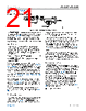
20 / 66 page  Data Sheet AD4052/AD4058 THEORY OF OPERATION analog.com Rev. B | 20 of 66 ANALOG INPUTS Figure 38. Equivalent Analog Input Circuit Figure 38 shows an equivalent circuit for each of the AD4052/ AD4058 analog inputs (IN+ and IN−). The analog inputs are mod- eled as a switched capacitive load. During the acquisition phase, the sampling switch (SW) connects each input pin to the 3.4 pF sampling capacitor (CIN) in series with the 230 Ω switch on resistance (RON). During the conversion phase, SW disconnects to sample the voltages on the IN+ and IN− pins onto the sampling capacitors. D1 and D2 represent the ESD diodes from the IN+ and IN− pins to the VDD supply and GND, respectively. CPIN represents the pin capacitance of each input pin to GND and is typically 2 pF. See the AD4052/AD4058 Equivalent Analog Input Model section for more information on the effective loading characteristics of the AD4052/AD4058 analog inputs. Easy Drive Features The AD4052/AD4058 Easy Drive analog inputs are designed to enable compact, low-power precision signal chains by minimizing dependence on specialized high-speed, low-noise, high-power ADC driver amplifiers. The small sampling capacitors minimize the transi- ent current glitches typical of SAR ADCs, and the long acquisition phase maximizes the settling time—even at high sample rates. The RC kickback filter uses smaller capacitors and larger resistors, alleviating amplifier stability concerns and enabling the use of tiny passive components (for example, 0201 NP0/C0G capacitors). These Easy Drive features ensure the AD4052/AD4058 interface with front-end circuits with high output impedance without incurring settling errors, expanding compatibility with low-power amplifiers and sensors (see the Analog Front-End Design section). The AD4052/AD4058 are available in the LTspice component library and support cosimulation with a wide variety of companion amplifi- ers. The LTspice model emulates the input-referred noise spectral density and input transient loading for system noise and settling accuracy simulations. VOLTAGE REFERENCE The VREF voltage sets the ADC FSR (see the Transfer Function section). The AD4052/AD4058 VREF range is 2.3 V to VDD, where the maximum VDD supply voltage is 3.6 V (see Table 1). The VREF voltage is polled during the SAR bit trials to determine the ADC output code. During the bit trials, the SAR core exhibits transient charge draw. To ensure the VREF voltage remains stable during the SAR bit trials, place a 2.2 μF decoupling capacitor as close to the REF pin as possible. Lower decoupling capacitance values (for example, 1 μF) may be used with slight performance degradations. See the Reference Circuit Design section for more recommendations for pairing voltage references with the AD4052/ AD4058. Reference Selection Modes The AD4052/AD4058 VREF voltage can be sourced from either the REF input pin or the VDD supply pin. By default, the REF pin acts as the VREF source, and this setting is the intended mode to achieve the performance specifications given in Table 1. The VDD supply option is provided to support low-power measurements where accuracy is not critical or to allow the system to power cycle the voltage reference for long periods of time to save system power. The VREF source option is controlled with the REF_SEL bit in the ADC_CONFIG register (see Table 39). The AD4052/AD4058 include an automated gain scaling function, where the ADC core samples the REF voltage as a fraction of the VDD supply voltage and stores the appropriate gain scaling value into the MON_VAL register, such that using VDD as the VREF source has the same ADC transfer function as REF. This allows the system to power down the voltage reference circuitry for extended periods of time with similar levels of performance. See the Achieving High Accuracy with Reference Shutdown section for a detailed description of the automated gain scaling feature. Figure 39. Reference Source Selection |
|
链接网址 |
| ALLDATASHEET是否为您带来帮助? [ DONATE ] |
关于 Alldatasheet | 广告服务 | 联系我们 | 隐私政策 | 数据表链接 | 链接交换 | 制造商名单 All Rights Reserved©Alldatasheet.com |
| Russian : Alldatasheetru.com | Korean : Alldatasheet.co.kr | Spanish : Alldatasheet.es | French : Alldatasheet.fr | Italian : Alldatasheetit.com Portuguese : Alldatasheetpt.com | Polish : Alldatasheet.pl | Vietnamese : Alldatasheet.vn Indian : Alldatasheet.in | Mexican : Alldatasheet.com.mx | British : Alldatasheet.co.uk | New Zealand : Alldatasheet.co.nz |
|
Family Site : ic2ic.com |
icmetro.com |
 Chinese ▼
 English
 Chinese
 German
 Japanese
 Russian
 Korean
 Spanish
 French
 Italian
 Portuguese
 Polish
 Vietnamese
 Indian
 Mexican
 British
 New Zealand