|
数据搜索系统,热门电子元器件搜索 |
|
|
数据搜索系统,热门电子元器件搜索 |
|
EM357-RTR 数据表(PDF) 160 Page - List of Unclassifed Manufacturers |
|
|
|||||||||||||||||||||||||||||
EM357-RTR 数据表(HTML) 160 Page - List of Unclassifed Manufacturers |
|
|
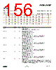
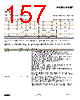
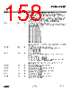
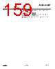
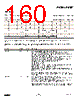
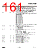
160 / 240 page  EM351 / EM357 TIMx_CCMR2 TIM1_CCMR2 Timer 1 Capture/Compare Mode Register 2 Address: 0x4000E01C Reset: 0x0 TIM2_CCMR2 Timer 2 Capture/Compare Mode Register 2 Address: 0x4000F01C Reset: 0x0 31 30 29 28 27 26 25 24 0 0 0 0 0 0 0 0 23 22 21 20 19 18 17 16 0 0 0 0 0 0 0 0 15 14 13 12 11 10 9 8 0 TIM_OC4M TIM_OC4BE TIM_OC4FE TIM_IC4F TIM_IC4PSC TIM_CC4S 7 6 5 4 3 2 1 0 0 TIM_OC3M TIM_OC3BE TIM_OC3FE TIM_IC3F TIM_IC3PSC TIM_CC3S Timer channels can be programmed as inputs (capture mode) or outputs (compare mode). The direction of channel y is defined by TIM_CCyS in this register. The other bits in this register have different functions in input and in output modes. The TIM_OC* fields only apply to a channel configured as an output (TIM_CCyS = 0), and the TIM_IC* fields only apply to a channel configured as an input (TIM_CCyS > 0). Bitname Bitfield Access Description TIM_OC4M [14:12] RW Output Compare 4 Mode. (Applies only if TIM_CC4S = 0.) Define the behavior of the output reference signal OC4REF from which OC4 derives. OC4REF is active high whereas OC4’s active level depends on the TIM_CC4P bit. 000: Frozen - The comparison between the output compare register TIMx_CCR4 and the counter TIMx_CNT has no effect on the outputs. 001: Set OC4REF to active on match. The OC4REF signal is forced high when the counter TIMx_CNT matches the capture/compare register 4 (TIMx_CCR4) 010: Set OC4REF to inactive on match. OC4REF signal is forced low when the counter TIMx_CNT matches the capture/compare register 4 (TIMx_CCR4). 011: Toggle - OC4REF toggles when TIMx_CNT = TIMx_CCR4. 100: Force OC4REF inactive. 101: Force OC4REF active. 110: PWM mode 1 - In up-counting, OC4REF is active as long as TIMx_CNT < TIMx_CCR4, otherwise OC4REF is inactive. In down-counting, OC4REF is inactive if TIMx_CNT > TIMx_CCR4, otherwise OC4REF is active. 111: PWM mode 2 - In up-counting, OC4REF is inactive if TIMx_CNT < TIMx_CCR4, otherwise OC4REF is active. In down-counting, OC4REF is active if TIMx_CNT > TIMx_CCR4, otherwise it is inactive. Note: In PWM mode 1 or 2, the OC4REF level changes only when the result of the comparison changes or when the output compare mode switches from “frozen” mode to “PWM” mode. TIM_OC4BE [11] RW Output Compare 4 Buffer Enable. (Applies only if TIM_CC4S = 0.) 0: Buffer register for TIMx_CCR4 is disabled. TIMx_CCR4 can be written at anytime, the new value is used by the shadow register immediately. 1: Buffer register for TIMx_CCR4 is enabled. Read/write operations access the buffer register. TIMx_CCR4 buffer value is loaded in the shadow register at each UEV. Note: The PWM mode can be used without enabling the buffer register only in one pulse mode (TIM_OPM bit set in the TIMx_CR2 register), otherwise the behavior is undefined. 9-40 120-035X-000D Preliminary |
|
链接网址 |
| ALLDATASHEET是否为您带来帮助? [ DONATE ] |
关于 Alldatasheet | 广告服务 | 联系我们 | 隐私政策 | 数据表链接 | 链接交换 | 制造商名单 All Rights Reserved©Alldatasheet.com |
| Russian : Alldatasheetru.com | Korean : Alldatasheet.co.kr | Spanish : Alldatasheet.es | French : Alldatasheet.fr | Italian : Alldatasheetit.com Portuguese : Alldatasheetpt.com | Polish : Alldatasheet.pl | Vietnamese : Alldatasheet.vn Indian : Alldatasheet.in | Mexican : Alldatasheet.com.mx | British : Alldatasheet.co.uk | New Zealand : Alldatasheet.co.nz |
|
Family Site : ic2ic.com |
icmetro.com |
 Chinese ▼
 English
 Chinese
 German
 Japanese
 Russian
 Korean
 Spanish
 French
 Italian
 Portuguese
 Polish
 Vietnamese
 Indian
 Mexican
 British
 New Zealand