|
数据搜索系统,热门电子元器件搜索 |
|
|
数据搜索系统,热门电子元器件搜索 |
|
PCMB065T-R68MS 数据表(PDF) 22 Page - International Rectifier |
|
|
|||||||||||||||||||||||||||||
PCMB065T-R68MS 数据表(HTML) 22 Page - International Rectifier |
|
|
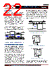
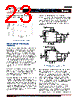
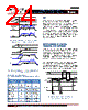
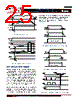
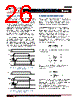
22 / 46 page  - 22 - JANURARY 18, 2013 | DATA SHEET | Rev 3.5 22 IR3898 6A Highly Integrated SupIRBuck TM Single-Input Voltage, Synchronous Buck Regulator PD-97662 FEEDFORWARD Feed-Forward (F.F.) is an important feature, because it can keep the converter stable and preserve its load transient performance when Vin varies in a large range. In IR3898, F.F. function is enabled when Vin pin is connected to PVin pin. In this case, the internal low dropout (LDO) regulator is used. The PWM ramp amplitude (Vramp) is proportionally changed with Vin to maintain Vin/Vramp almost constant throughout Vin variation range (as shown in Fig. 10). Thus, the control loop bandwidth and phase margin can be maintained constant. Feed-forward function can also minimize impact on output voltage from fast Vin change. The maximum Vin slew rate is within 1V/µs. If an external bias voltage is used as Vcc, Vin pin should be connected to Vcc/LDO_Out pin instead of PVin pin. Then the F.F. function is disabled. A re-calculation of control loop parameters is needed for re-compensation. 0 0 Vin PWM Ramp 12V Ramp Offset 21V 6.8V 12V PWM Ramp Amplitude = 1.8V PWM Ramp Amplitude = 3.15V PWM Ramp Amplitude = 1.02V PWM Ramp Amplitude = 0.15xVin Figure 10: Timing Diagram for Feed-Forward (F.F.) Function SMART LOW DROPOUT REGULATOR (LDO) IR3898 has an integrated low dropout (LDO) regulator which can provide gate drive voltage for both drivers. In order to improve overall efficiency over the entire load range, LDO voltage is set to 6.4V (typ.) at mid- or heavy load condition to reduce Rds(on) and thus MOSFET conduction loss; and it is reduced to 4.4 (typ.) at light load condition to reduce gate drive loss. The smart LDO can select its output voltage according to the load condition by sensing switch node (SW) voltage. At light load condition when part of the inductor current flows in the reverse direction (DCM=1), VSW > 0 on LDrv falling edge in a switching cycle. If this case happens for consecutive 256 switching cycles, the smart LDO reduces its output to 4.4. If in any one of the 256 cycles, Vsw < 0 on LDrv falling edge, the counter is reset and LDO voltage doesn’t change. On the other hand, if Vsw < 0 on LDrv falling edge (DCM=0), LDO output is increased to 6.4V. A hysteresis band is added to Vsw comparison to avoid chattering. Figure 11a shows the timing diagram. Whenever device turns on, LDO always starts with 6.4V, then goes to 4.4V/6.4V depending upon the load condition. For internally biased single rail operation, Vin pin should be connected to PVin pin, as shown in Figure 11b. If external bias voltage is used, Vin pin should be connected to Vcc/LDO_Out pin, as shown in Figure 11c. Vcc/ LDO 0 0 IL 256/Fs ... ... ... 6.4V 6.4V 4.4V ... Figure 11a: Time Diagram for Smart LDO IR3898 VCC/ LDO_OUT PGnd Vin Vin PVin Figure 11b: Internally Biased Single Rail Operation Ext VCC Vin IR3898 VCC/ LDO_OUT PGnd Vin PVin Figure 11c: Use External Bias Voltage When the Vin voltage is below 6.8V, the internal LDO enters the dropout mode at medium and heavy load. The dropout voltage increases with the switching frequency. Figure 11d |
|
链接网址 |
| ALLDATASHEET是否为您带来帮助? [ DONATE ] |
关于 Alldatasheet | 广告服务 | 联系我们 | 隐私政策 | 数据表链接 | 链接交换 | 制造商名单 All Rights Reserved©Alldatasheet.com |
| Russian : Alldatasheetru.com | Korean : Alldatasheet.co.kr | Spanish : Alldatasheet.es | French : Alldatasheet.fr | Italian : Alldatasheetit.com Portuguese : Alldatasheetpt.com | Polish : Alldatasheet.pl | Vietnamese : Alldatasheet.vn Indian : Alldatasheet.in | Mexican : Alldatasheet.com.mx | British : Alldatasheet.co.uk | New Zealand : Alldatasheet.co.nz |
|
Family Site : ic2ic.com |
icmetro.com |
 Chinese ▼
 English
 Chinese
 German
 Japanese
 Russian
 Korean
 Spanish
 French
 Italian
 Portuguese
 Polish
 Vietnamese
 Indian
 Mexican
 British
 New Zealand