|
数据搜索系统,热门电子元器件搜索 |
|
|
数据搜索系统,热门电子元器件搜索 |
|
PCMB065T-R68MS 数据表(PDF) 41 Page - International Rectifier |
|
|
|||||||||||||||||||||||||||||
PCMB065T-R68MS 数据表(HTML) 41 Page - International Rectifier |
|
|
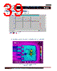
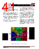
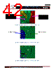
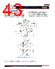
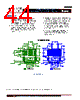
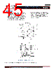
41 / 46 page  - 41 - JANURARY 18, 2013 | DATA SHEET | Rev 3.5 41 IR3898 6A Highly Integrated SupIRBuck TM Single-Input Voltage, Synchronous Buck Regulator PD-97662 LAYOUT RECOMMENDATIONS The layout is very important when designing high frequency switching converters. Layout will affect noise pickup and can cause a good design to perform with less than expected results. Make the connections for the power components in the top layer with wide, copper filled areas or polygons. In general, it is desirable to make proper use of power planes and polygons for power distribution and heat dissipation. The inductor, output capacitors and the IR3898 should be as close to each other as possible. This helps to reduce the EMI radiated by the power traces due to the high switching currents through them. Place the input capacitor directly at the PVin pin of IR3898. The feedback part of the system should be kept away from the inductor and other noise sources. The critical bypass components such as capacitors for Vin, Vcc and Vref should be close to their respective pins. It is important to place the feedback components including feedback resistors and compensation components close to Fb and Comp pins. In a multilayer PCB use one layer as a power ground plane and have a control circuit ground (analog ground), to which all signals are referenced. The goal is to localize the high current path to a separate loop that does not interfere with the more sensitive analog control function. These two grounds must be connected together on the PC board layout at a single point. It is recommended to place all the compensation parts over the analog ground plane in top layer. The Power QFN is a thermally enhanced package. Based on thermal performance it is recommended to use at least a 4-layers PCB. To effectively remove heat from the device the exposed pad should be connected to the ground plane using vias. Figures 46a-d illustrates the implementation of the layout guidelines outlined above, on the IRDC3898 4- layer demo board. Figure 49a: IRDC3898 Demo board Layout Considerations – Top Layer Compensation parts should be placed as close as possible to the Comp pin Resistor Rt and Vref decoupling cap should be placed as close as possible to their pins Enough copper & minimum ground length path between Input and Output All bypass caps should be placed as close as possible to their connecting pins SW node copper is kept only at the top layer to minimize the switching noise |
|
链接网址 |
| ALLDATASHEET是否为您带来帮助? [ DONATE ] |
关于 Alldatasheet | 广告服务 | 联系我们 | 隐私政策 | 数据表链接 | 链接交换 | 制造商名单 All Rights Reserved©Alldatasheet.com |
| Russian : Alldatasheetru.com | Korean : Alldatasheet.co.kr | Spanish : Alldatasheet.es | French : Alldatasheet.fr | Italian : Alldatasheetit.com Portuguese : Alldatasheetpt.com | Polish : Alldatasheet.pl | Vietnamese : Alldatasheet.vn Indian : Alldatasheet.in | Mexican : Alldatasheet.com.mx | British : Alldatasheet.co.uk | New Zealand : Alldatasheet.co.nz |
|
Family Site : ic2ic.com |
icmetro.com |
 Chinese ▼
 English
 Chinese
 German
 Japanese
 Russian
 Korean
 Spanish
 French
 Italian
 Portuguese
 Polish
 Vietnamese
 Indian
 Mexican
 British
 New Zealand