|
数据搜索系统,热门电子元器件搜索 |
|
|
数据搜索系统,热门电子元器件搜索 |
|
PCMB065T-R68MS 数据表(PDF) 30 Page - International Rectifier |
|
|
|||||||||||||||||||||||||||||
PCMB065T-R68MS 数据表(HTML) 30 Page - International Rectifier |
|
|
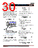
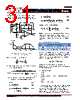
30 / 46 page  - 30 - JANURARY 18, 2013 | DATA SHEET | Rev 3.5 30 IR3898 6A Highly Integrated SupIRBuck TM Single-Input Voltage, Synchronous Buck Regulator PD-97662 The IR3898 uses a voltage-type error amplifier with high-gain (110dB) and high-bandwidth (30MHz). The output of the amplifier is available for DC gain control and AC phase compensation. The error amplifier can be compensated either in type II or type III compensation. Type II compensation is shown in Fig. 26. This method requires that the output capacitors have enough ESR to satisfy stability requirements. If the output capacitor’s ESR generates a zero at 5kHz to 50kHz, the zero generates acceptable phase margin and the Type II compensator can be used. The ESR zero of the output capacitor is expressed as follows: 1 (18) 2 ESR o F π* ESR* C VOUT VREF R6 R5 C POLE C3 R3 Ve FZ F POLE E/A Z f Frequency Gain(dB) H(s) dB Fb Comp Z IN Figure 26: Type II compensation network and its asymptotic gain plot The transfer function (Ve/Vout) is given by: 3 3 5 3 1 ( ) (19) f e out IN Z V sR C Hs V Z sR C The (s) indicates that the transfer function varies as a function of frequency. This configuration introduces a gain and zero, expressed by: 3 5 3 3 (20) 1 (21) 2 * * z R Hs R F RC First select the desired zero-crossover frequency (Fo): o (22) and F 1/5~1/10 * o ESR s F F F Use the following equation to calculate R3: 5 3 2 * * * (23) * osc o ESR in LC V F F R R VF Where: Vin = Maximum Input Voltage Vosc = Amplitude of the oscillator Ramp Voltage Fo = Crossover Frequency FESR = Zero Frequency of the Output Capacitor FLC = Resonant Frequency of the Output Filter R5 = Feedback Resistor To cancel one of the LC filter poles, place the zero before the LC filter resonant frequency pole: 75 % * 1 0.75* (24) 2* z LC z oo FF F LC Use equations (20), (21) and (22) to calculate C3. One more capacitor is sometimes added in parallel with C3 and R3. This introduces one more pole which is mainly used to suppress the switching noise. The additional pole is given by: 3 3 3 1 (25) * 2 * * P POLE POLE F CC R CC The pole sets to one half of the switching frequency which results in the capacitor CPOLE: 3 3 3 11 (26) 1 POLE s s C * R * F * R * F C |
|
链接网址 |
| ALLDATASHEET是否为您带来帮助? [ DONATE ] |
关于 Alldatasheet | 广告服务 | 联系我们 | 隐私政策 | 数据表链接 | 链接交换 | 制造商名单 All Rights Reserved©Alldatasheet.com |
| Russian : Alldatasheetru.com | Korean : Alldatasheet.co.kr | Spanish : Alldatasheet.es | French : Alldatasheet.fr | Italian : Alldatasheetit.com Portuguese : Alldatasheetpt.com | Polish : Alldatasheet.pl | Vietnamese : Alldatasheet.vn Indian : Alldatasheet.in | Mexican : Alldatasheet.com.mx | British : Alldatasheet.co.uk | New Zealand : Alldatasheet.co.nz |
|
Family Site : ic2ic.com |
icmetro.com |
 Chinese ▼
 English
 Chinese
 German
 Japanese
 Russian
 Korean
 Spanish
 French
 Italian
 Portuguese
 Polish
 Vietnamese
 Indian
 Mexican
 British
 New Zealand