|
数据搜索系统,热门电子元器件搜索 |
|
|
数据搜索系统,热门电子元器件搜索 |
|
PCMB065T-R68MS 数据表(PDF) 31 Page - International Rectifier |
|
|
|||||||||||||||||||||||||||||
PCMB065T-R68MS 数据表(HTML) 31 Page - International Rectifier |
|
|
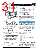
31 / 46 page  - 31 - JANURARY 18, 2013 | DATA SHEET | Rev 3.5 31 IR3898 6A Highly Integrated SupIRBuck TM Single-Input Voltage, Synchronous Buck Regulator PD-97662 For a general solution for unconditional stability for any type of output capacitors, and a wide range of ESR values, a type III compensation network can be used, as shown in Fig. 27. VOUT VREF R6 R5 R4 C4 C2 C3 R3 Ve FZ 1 FZ 2 FP 2 FP 3 E / A Zf ZIN Frequency Gain (dB) |H(s)| dB Fb Comp Figure 27: Type III Compensation network and its asymptotic gain plot Again, the transfer function is given by: IN f out e Z Z s H V V ) ( By replacing Zin and Zf, according to Fig. 27, the transfer function can be expressed as: 3 3 4 4 5 23 5 2 3 3 4 4 23 (1 ) 1 * ( ) ( ) 1 (1 ) (27) sR C sC R R CC Hs sR C C sR sR C CC The compensation network has three poles and two zeros and they are expressed as follows: 1 2 44 3 32 23 3 23 0 (28) 1 (29) 2 * * 11 (30) 2 * * * 2* P P P F F RC F RC CC R CC 1 33 2 4 4 5 4 5 1 (31) 2 * * 11 (32) 2 * *( ) 2 * * Z Z F RC F C R R C R Crossover frequency is expressed as: 34 1 * * * (33) 2 * * in o osc o o V F R C V L C Based on the frequency of the zero generated by the output capacitor and its ESR, relative to crossover frequency, the compensation type can be different. Table 3 shows the compensation types for relative locations of the crossover frequency. TABLE 3: DIFFERENT TYPES OF COMPENSATORS Compensator Type FESR vs FO Typical Output Capacitor Type II FLC < FESR < FO < FS/2 Electrolytic Type III FLC < FO < FESR SP Cap, Ceramic The higher the crossover frequency is, the potentially faster the load transient response will be. However, the crossover frequency should be low enough to attenuate the switching noise. Typically, the control loop bandwidth or crossover frequency (Fo) is selected such that: s o F F * 1/10 ~ 1/5 The DC gain should be large enough to provide high DC-regulation accuracy. The phase margin should be greater than 45 o for overall stability. For this design we have: Vin=12V Vo=1.2V Vosc=1.8V (This is a function of Vin, see feedforward section) Vref=0.5V Lo=1.0uH Co=4x22uF, ESR≈3mΩ each It must be noted here that the value of the capacitance used in the compensator design must be the small signal value. For instance, the small signal capacitance of the 22uF capacitor used in this design is 10uF at 1.2 V DC bias and 600 kHz frequency. It is this value that must be used for all computations related to the compensation. The small signal |
|
链接网址 |
| ALLDATASHEET是否为您带来帮助? [ DONATE ] |
关于 Alldatasheet | 广告服务 | 联系我们 | 隐私政策 | 数据表链接 | 链接交换 | 制造商名单 All Rights Reserved©Alldatasheet.com |
| Russian : Alldatasheetru.com | Korean : Alldatasheet.co.kr | Spanish : Alldatasheet.es | French : Alldatasheet.fr | Italian : Alldatasheetit.com Portuguese : Alldatasheetpt.com | Polish : Alldatasheet.pl | Vietnamese : Alldatasheet.vn Indian : Alldatasheet.in | Mexican : Alldatasheet.com.mx | British : Alldatasheet.co.uk | New Zealand : Alldatasheet.co.nz |
|
Family Site : ic2ic.com |
icmetro.com |
 Chinese ▼
 English
 Chinese
 German
 Japanese
 Russian
 Korean
 Spanish
 French
 Italian
 Portuguese
 Polish
 Vietnamese
 Indian
 Mexican
 British
 New Zealand