|
数据搜索系统,热门电子元器件搜索 |
|
|
数据搜索系统,热门电子元器件搜索 |
|
PCMB065T-R68MS 数据表(PDF) 32 Page - International Rectifier |
|
|
|||||||||||||||||||||||||||||
PCMB065T-R68MS 数据表(HTML) 32 Page - International Rectifier |
|
|
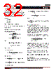
32 / 46 page  - 32 - JANURARY 18, 2013 | DATA SHEET | Rev 3.5 32 IR3898 6A Highly Integrated SupIRBuck TM Single-Input Voltage, Synchronous Buck Regulator PD-97662 value may be obtained from the manufacturer’s datasheets, design tools or SPICE models. Alternatively, they may also be inferred from measuring the power stage transfer function of the converter and measuring the double pole frequency FLC and using equation (17) to compute the small signal Co. These result in: FLC=25.2 kHz FESR=5.3 MHz Fs/2=300 kHz Select crossover frequency F0=120 kHz Since FLC<F0<Fs/2<FESR, Type III is selected to place the pole and zeros. Detailed calculation of compensation Type III: Desired Phase Boost Θ = 70° 2 1 sin 21.2 kHz 1 sin Zo FF 2 1 sin 680.6 kHz 1 sin Po FF Select: 12 0.5* 10.6 kHz and ZZ FF 3 0.5* 300 kHz Ps FF Select C4 = 2.2nF. Calculate R3, C3 and C2: 33 4 2 * * * * ; 2.1 kΩ * o o o osc in F L C V RR CV Select R3 = 2.0 kΩ: 3 3 3 1 3 1 ; 7.5 nF, Select: 10 nF 2 * * Z C C C FR 2 2 2 33 1 ; 265 pF, Select: 180 pF 2 * * P C C C FR Calculate R4, R5 and R6: 4 4 4 42 1 ; 106 Ω, Select: 100 Ω 2 * * P R R R CF 5 4 5 42 1 - ; 3.41 kΩ, 2 * * Z R R R CF Select R5 = 3.32 kΩ: 6 5 6 6 * ; 2.37 kΩ Select: 2.37 kΩ - ref o ref V R R R R VV Setting the Power Good Threshold In this design IR3898 is used in normal (non-tracking, non-sequencing) mode, therefore the PGood thresholds are internally set at 90% and 120% of Vref. At startup as soon as Vsns voltage reaches 0.9*0.5V=0.45V (Fig. 15), after 1.28ms delay, PGood signal is asserted. As long as the Vsns voltage is between the threshold range, Enable is high, and no fault happens, the PGood remains high. The following formula can be used to set the threshold. VoutPGood_Th can be taken as 90% of Vout. Choose R7=3.32KΩ: _ * 0.9 * 7 8 (34) * 0.9 8 2.37 PGood Th Vref R R Vout Vref RK The PGood is an open drain output. Hence, it is necessary to use a pull up resistor, RPG, from PGood pin to Vcc. The value of the pull-up resistor must be chosen such as to limit the current flowing into the PGood pin to less than 5mA when the output voltage is not in regulation. A typical value used is 49.9kΩ. OVP comparator also uses Vsns signal for over Voltage dectection.With above values for R7 and R8, OVP trip point (Vout_OVP) is _ *1.2*( 7 8) / 8 1.44 (35) OVP Vout Vref R R R V Vref Bypass Capacitor A 100pF bypass capacitor is recommended to be placed between Vref and Gnd pins.This capacitor should be placed as close as possible to Vref pin. |
|
链接网址 |
| ALLDATASHEET是否为您带来帮助? [ DONATE ] |
关于 Alldatasheet | 广告服务 | 联系我们 | 隐私政策 | 数据表链接 | 链接交换 | 制造商名单 All Rights Reserved©Alldatasheet.com |
| Russian : Alldatasheetru.com | Korean : Alldatasheet.co.kr | Spanish : Alldatasheet.es | French : Alldatasheet.fr | Italian : Alldatasheetit.com Portuguese : Alldatasheetpt.com | Polish : Alldatasheet.pl | Vietnamese : Alldatasheet.vn Indian : Alldatasheet.in | Mexican : Alldatasheet.com.mx | British : Alldatasheet.co.uk | New Zealand : Alldatasheet.co.nz |
|
Family Site : ic2ic.com |
icmetro.com |
 Chinese ▼
 English
 Chinese
 German
 Japanese
 Russian
 Korean
 Spanish
 French
 Italian
 Portuguese
 Polish
 Vietnamese
 Indian
 Mexican
 British
 New Zealand