|
数据搜索系统,热门电子元器件搜索 |
|
|
数据搜索系统,热门电子元器件搜索 |
|
PCMB065T-R68MS 数据表(PDF) 24 Page - International Rectifier |
|
|
|||||||||||||||||||||||||||||
PCMB065T-R68MS 数据表(HTML) 24 Page - International Rectifier |
|
|
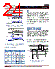
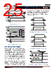
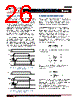
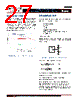
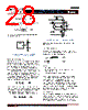
24 / 46 page  - 24 - JANURARY 18, 2013 | DATA SHEET | Rev 3.5 24 IR3898 6A Highly Integrated SupIRBuck TM Single-Input Voltage, Synchronous Buck Regulator PD-97662 Vcc Vref=0.5V 1.2V Soft Start (slave) Enable (slave) Vo1 (master) Vo2 (slave) (a) Vo1 (master) Vo2 (slave) (b) Figure 13: Typical waveforms for sequencing mode of operation: (a) simultaneous, (b) ratiometric Vcc Vref=0V (slave) 1.2V Soft Start (slave) Enable (slave) Vo1 (master) Vo2 (slave) (a) Vo1 (master) Vo2 (slave) (b) Figure 14: Typical waveforms in tracking mode of operation: (a) simultaneous, (b) ratiometric TABLE 2: REQUIRED CONDITIONS FOR SIMULTANEOUS/RATIOMETRIC TRACKING AND SEQUENCING (FIG. 12) Operating Mode Vref (Slave) Vp Required Condition Normal (Non-sequencing, Non-tracking) 0.5V (Floating) Floating ― Simultaneous Sequencing 0.5V Ramp up from 0V RA/RB>RE/ RF=RC/RD Ratiometric Sequencing 0.5V Ramp up from 0V RA/RB>RE/ RF>RC/RD Simultaneous Tracking 0V Ramp up before En RE/RF =RC/RD Ratiometric Tracking 0V Ramp up before En RE/RF >RC/RD VREF This pin reflects the internal reference voltage which is used by the error amplifier to set the output voltage. In most operating conditions this pin is only connected to an external bypass capacitor and it is left floating. A 100pF ceramic capacitor is recommended for the bypass capacitor. To keep stand by current to minimum, Vref is not allowed to come up until EN starts going high. In tracking mode this pin should be pulled to GND. For margining applications, an external voltage source is connected to Vref pin and overrides the internal reference voltage. The external voltage source should have a low internal resistance (<100Ω) and be able to source and sink more than 25µA. POWER GOOD OUTPUT (TRACKING, SEQUENCING, VREF MARGINING) IR3898 continually monitors the output voltage via the sense pin (Vsns) voltage. The Vsns voltage is an input to the window comparator with upper and lower threshold of 0.6V and 0.45V respectively. PGood signal is high whenever Vsns voltage is within the PGood comparator window thresholds. The PGood pin is open drain and it needs to be externally pulled high. High state indicates that output is in regulation. The threshold is set differently at different operating modes and the results of the comparison sets the PGood signal. Figures 15, 16, and 17 show the timing diagram of the PGood signal at different operating modes. Vsns signal is also used by OVP comparator for detecting output over voltage condition. 0 0 0 Vref PGood Vsns 0.5 V 1.2*Vref 0.85*Vp 1.28ms 1.28ms OVP Latch 0.9*Vp Figure 15: Non-sequence, Non-tracking Startup and Vref Margin (Vp pin floating) |
|
链接网址 |
| ALLDATASHEET是否为您带来帮助? [ DONATE ] |
关于 Alldatasheet | 广告服务 | 联系我们 | 隐私政策 | 数据表链接 | 链接交换 | 制造商名单 All Rights Reserved©Alldatasheet.com |
| Russian : Alldatasheetru.com | Korean : Alldatasheet.co.kr | Spanish : Alldatasheet.es | French : Alldatasheet.fr | Italian : Alldatasheetit.com Portuguese : Alldatasheetpt.com | Polish : Alldatasheet.pl | Vietnamese : Alldatasheet.vn Indian : Alldatasheet.in | Mexican : Alldatasheet.com.mx | British : Alldatasheet.co.uk | New Zealand : Alldatasheet.co.nz |
|
Family Site : ic2ic.com |
icmetro.com |
 Chinese ▼
 English
 Chinese
 German
 Japanese
 Russian
 Korean
 Spanish
 French
 Italian
 Portuguese
 Polish
 Vietnamese
 Indian
 Mexican
 British
 New Zealand