|
数据搜索系统,热门电子元器件搜索 |
|
|
数据搜索系统,热门电子元器件搜索 |
|
PCMB065T-R68MS 数据表(PDF) 23 Page - International Rectifier |
|
|
|||||||||||||||||||||||||||||
PCMB065T-R68MS 数据表(HTML) 23 Page - International Rectifier |
|
|
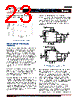
23 / 46 page  - 23 - JANURARY 18, 2013 | DATA SHEET | Rev 3.5 23 IR3898 6A Highly Integrated SupIRBuck TM Single-Input Voltage, Synchronous Buck Regulator PD-97662 shows the LDO voltage for 600 kHz and 1500 kHz switching frequency respectively. Figure 11d: LDO dropout Voltage OUTPUT VOLTAGE TRACKING AND SEQUENCING IR3898 can accommodate user programmable tracking and/or sequencing options using Vp, Vref, Enable, and Power Good pins. In the block diagram presented on page 3, the error-amplifier (E/A) has been depicted with three positive inputs. Ideally, the input with the lowest voltage is used for regulating the output voltage and the other two inputs are ignored. In practice the voltage of the other two inputs should be about 200mV greater than the low-voltage input so that their effects can completely be ignored. Vp is internally biased to 3.3V via a high impedance path. For normal operation, Vp and Vref is left floating (Vref should have a bypass capacitor). Therefore, in normal operating condition, after Enable goes high, the internal soft-start (Intl_SS) ramps up the output voltage until Vfb (voltage of feedback/Fb pin) reaches about 0.5V. Then Vref takes over and the output voltage is regulated. Tracking-mode operation is achieved by connecting Vref to GND. In tracking-mode, Vfb always follows Vp, which means Vout is always proportional to Vp voltage (typical for DDR/VTT rail applications). The effective Vp variation range is 0V~1.2V. Fig. 5c illustrates the start-up of VTT tracking for DDR4 application. Vp is proportional to VDDQ. After Vp is established, asserting Enable initiates the internal soft-start. VTT, which is the output of POL, starts to ramp up and tracks Vp. In sequencing mode of operation (simultaneous or ratiometric), Vref is left floating and Vp is kept to ground level until Intl_SS signal reaches the final value. Then Vp is ramped up and Vfb follows Vp. When Vp>0.5V the error-amplifier switches to Vref and the output voltage is regulated with Vref.The final Vp voltage after sequencing startup should between 0.7V ~ 3.3V. Boot Vcc/LDO Fb Comp Gnd PGnd SW Vo1 (master) PGood PGood Rt/ Sync 5 V <Vin<16V PVin Vp S_Ctrl Vin Vref EN RA RB Vsns Boot Vcc/LDO Fb Comp Gnd PGnd SW Vo2 (Salve) PGood PGood Rt/ Sync PVin Vp Vo1 (master) S_Ctrl Vin Vref EN RE RF RC RD 5 V < Vin < 16 V Vsns Figure 12: Application Circuit for Simultaneous and Ratiometric Sequencing Tracking and sequencing operations can be implemented to be simultaneous or ratiometric (refer to Fig. 13 and 14). Figure 12 shows typical circuit configuration for sequencing operation. With this power-up configuration, the voltage at the Vp pin of the slave reaches 0.5V before the Fb pin of the master. If RE/RF =RC/RD, simultaneous startup is achieved. That is, the output voltage of the slave follows that of the master until the voltage at the Vp pin of the slave reaches 0.5 V. After the voltage at the Vp pin of the slave exceeds 0.5V, the internal 0.5V reference of the slave dictates its output voltage. In reality the regulation gradually shifts from Vp to internal Vref. The circuit shown in Fig. 12 can also be used for simultaneous or ratiometric tracking operation if Vref of the slave is connected to GND. Table 2 summarizes the required conditions to achieve simultaneous/ratiometric tracking or sequencing operations. |
|
链接网址 |
| ALLDATASHEET是否为您带来帮助? [ DONATE ] |
关于 Alldatasheet | 广告服务 | 联系我们 | 隐私政策 | 数据表链接 | 链接交换 | 制造商名单 All Rights Reserved©Alldatasheet.com |
| Russian : Alldatasheetru.com | Korean : Alldatasheet.co.kr | Spanish : Alldatasheet.es | French : Alldatasheet.fr | Italian : Alldatasheetit.com Portuguese : Alldatasheetpt.com | Polish : Alldatasheet.pl | Vietnamese : Alldatasheet.vn Indian : Alldatasheet.in | Mexican : Alldatasheet.com.mx | British : Alldatasheet.co.uk | New Zealand : Alldatasheet.co.nz |
|
Family Site : ic2ic.com |
icmetro.com |
 Chinese ▼
 English
 Chinese
 German
 Japanese
 Russian
 Korean
 Spanish
 French
 Italian
 Portuguese
 Polish
 Vietnamese
 Indian
 Mexican
 British
 New Zealand