|
数据搜索系统,热门电子元器件搜索 |
|
|
数据搜索系统,热门电子元器件搜索 |
|
TMS320C31PQL60 数据表(PDF) 5 Page - Texas Instruments |
|
|
|||||||||||||||||||||||||||||
TMS320C31PQL60 数据表(HTML) 5 Page - Texas Instruments |
|
|
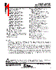
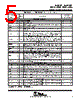
5 / 48 page  TMS320C31, TMS320LC31 DIGITAL SIGNAL PROCESSORS SPRS035B – MARCH 1996 – REVISED JANUARY 1999 5 POST OFFICE BOX 1443 • HOUSTON, TEXAS 77251–1443 TMS320C31 and TMS320LC31 Terminal Functions TERMINAL TYPE† DESCRIPTION CONDITIONS WHEN NAME QTY TYPE† DESCRIPTION WHEN SIGNAL IS Z TYPE‡ PRIMARY-BUS INTERFACE D31 – D0 32 I/O/Z 32-bit data port S H R A23 – A0 24 O/Z 24-bit address port S H R R/W 1 O/Z Read / write. R / W is high when a read is performed and low when a write is performed over the parallel interface. S H R STRB 1 O/Z External-access strobe S H RDY 1 I Ready. RDY indicates that the external device is prepared for a transaction completion. HOLD 1 I Hold. When HOLD is a logic low, any ongoing transaction is completed. A23 – A0, D31–D0, STRB, and R / W are placed in the high-impedance state and all transactions over the primary-bus interface are held until HOLD becomes a logic high or until the NOHOLD bit of the primary-bus-control register is set. HOLDA 1 O/Z Hold acknowledge. HOLDA is generated in response to a logic low on HOLD. HOLDA indicates that A23–A0, D31–D0, STRB, and R / W are in the high-impedance state and that all transactions over the bus are held. HOLDA is high in response to a logic high of HOLD or the NOHOLD bit of the primary-bus-control register is set. S CONTROL SIGNALS RESET 1 I Reset. When RESET is a logic low, the device is in the reset condition. When RESET becomes a logic high, execution begins from the location specified by the reset vector. INT3 – INT0 4 I External interrupts IACK 1 O/Z Interrupt acknowledge. IACK is generated by the IACK instruction. IACK can be used to indicate the beginning or the end of an interrupt-service routine. S MCBL / MP 1 I Microcomputer boot-loader / microprocessor mode-select SHZ 1 I Shutdown high impedance. When active, SHZ shuts down the device and places all pins in the high-impedance state. SHZ is used for board-level testing to ensure that no dual-drive conditions occur. CAUTION: A low on SHZ corrupts the device memory and register contents. Reset the device with SHZ high to restore it to a known operating condition. XF1, XF0 2 I/O/Z External flags. XF1 and XF0 are used as general-purpose I / Os or to support interlocked processor instruction. S R SERIAL PORT 0 SIGNALS CLKR0 1 I/O/Z Serial port 0 receive clock. CLKR0 is the serial shift clock for the serial port 0 receiver. S R CLKX0 1 I/O/Z Serial port 0 transmit clock. CLKX0 is the serial shift clock for the serial port 0 transmitter. S R DR0 1 I/O/Z Data-receive. Serial port 0 receives serial data on DR0. S R DX0 1 I/O/Z Data-transmit output. Serial port 0 transmits serial data on DX0. S R FSR0 1 I/O/Z Frame-synchronization pulse for receive. The FSR0 pulse initiates the data-receive process using DR0. S R FSX0 1 I/O/Z Frame-synchronization pulse for transmit. The FSX0 pulse initiates the data-transmit process using DX0. S R TIMER SIGNALS TCLK0 1 I/O/Z Timer clock 0. As an input, TCLK0 is used by timer 0 to count external pulses. As an output, TCLK0 outputs pulses generated by timer 0. S R TCLK1 1 I/O/Z Timer clock 1. As an input, TCLK0 is used by timer 1 to count external pulses. As an output, TCLK1 outputs pulses generated by timer 1. S R † I = input, O = output, Z = high-impedance state ‡ S = SHZ active, H = HOLD active, R = RESET active |
|
链接网址 |
| ALLDATASHEET是否为您带来帮助? [ DONATE ] |
关于 Alldatasheet | 广告服务 | 联系我们 | 隐私政策 | 数据表链接 | 链接交换 | 制造商名单 All Rights Reserved©Alldatasheet.com |
| Russian : Alldatasheetru.com | Korean : Alldatasheet.co.kr | Spanish : Alldatasheet.es | French : Alldatasheet.fr | Italian : Alldatasheetit.com Portuguese : Alldatasheetpt.com | Polish : Alldatasheet.pl | Vietnamese : Alldatasheet.vn Indian : Alldatasheet.in | Mexican : Alldatasheet.com.mx | British : Alldatasheet.co.uk | New Zealand : Alldatasheet.co.nz |
|
Family Site : ic2ic.com |
icmetro.com |
 Chinese ▼
 English
 Chinese
 German
 Japanese
 Russian
 Korean
 Spanish
 French
 Italian
 Portuguese
 Polish
 Vietnamese
 Indian
 Mexican
 British
 New Zealand