|
数据搜索系统,热门电子元器件搜索 |
|
|
数据搜索系统,热门电子元器件搜索 |
|
AD9739-R2-EBZ 数据表(PDF) 27 Page - Analog Devices |
|
|
|||||||||||||||||||||||||||||
AD9739-R2-EBZ 数据表(HTML) 27 Page - Analog Devices |
|
|
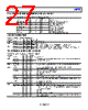
27 / 50 page  Data Sheet AD9739 Rev. E | Page 27 of 50 SYNC AND DATA RECEIVER CONTROLLER LOCK/TRACKING STATUS Table 22. Sync and Data Receiver Controller Lock/Tracking Status Register Address (Hex) Name Bit R/W Default Setting Comments 0x21 SYNC_TRK_ON 7 R 0 SYNC_TRK_ON and RCVR_TRK_ON: 0 = tracking not established. 1 = tracking established. SYNC_LCK and RCVR_LCK: 0 = controller is not locked. 1 = controller is locked. SYNC_LST and RCVR_LST: 0 = lock has not been lost. 1 = lock has been lost at some point. SYNC_LST 5 R 0 SYNC_LCK 4 R 0 RCVR_TRK_ON 3 R 0 RCVR_LST 1 R 0 RCVR_LCK 0 R 0 CLK INPUT COMMON MODE Table 23. CLK Input Common Mode Register Address (Hex) Name Bit R/W Default Setting Comments 0x22 DIR_P 4 R/W 0 DIR_P and DIR_N: 0 = VCM at the DACCLK_P input decreases with the offset value. 1 = VCM at the DACCLK_P input increases with the offset value. CLKx_OFFSET sets the magnitude of the offset for the DACCLK_P and DACCLK_N inputs. For optimum performance, set to 1111. CLKP_OFFSET[3:0] [3:0] R/W 0000 0x23 DIR_N 4 R/W 0 CLKN_OFFSET[3:0] [3:0] R/W 0000 MU CONTROLLER CONFIGURATION AND STATUS Table 24. Mu Controller Configuration and Status Register Address (Hex) Name Bit R/W Default Setting Comments 0x24 CMP_BST 5 R/W 0 Phase detector enable and boost bias bits. Note that both bits should always be set to 1 to enable these functions. PHS_DET AUTO_EN 4 R/W 0 0x25 MU_DUTY AUTO_EN 7 R/W 0 Mu controller duty cycle enable. Note that this bit should always be set to 1 to enable. 0x26 Slope 6 R/W 1 Mu controller phase slope lock. 0 = negative slope, 1 = positive slope. Refer to Table 28 for optimum setting. Mode[1:0] [5:4] R/W 00 Sets the mu controller mode of operation. 00 = search and track (recommended). 01 = search only. 10 = track. Read 3 R/W 0 Set to 1 to read the current value of the mu delay line in. Gain[1:0] [2:1] R/W 01 Sets the mu controller tracking gain. Recommended to leave at the default 01 setting. Enable 0 R/W 0 1 = enable the mu controller. 0 = disable the mu controller. 0x27 MUDEL[0] 7 R/W 0 The LSB of the 9-bit MUDEL setting. SRCH_MODE[1:0] [6:5] R/W 0 Sets the direction in which the mu controller searches (from its initial MUDEL setting) for the optimum mu delay line setting that corresponds to the desired phase/slope setting (that is, SET_PHS and slope ). 00 = down. 01 = up. 10 = down/up (recommended). SET_PHS[4:0] [4:0] R/W 0 Sets the target phase that the mu controller locks to with a maximum setting of 16. Refer to Table 28 for optimum setting. |
|
链接网址 |
| ALLDATASHEET是否为您带来帮助? [ DONATE ] |
关于 Alldatasheet | 广告服务 | 联系我们 | 隐私政策 | 数据表链接 | 链接交换 | 制造商名单 All Rights Reserved©Alldatasheet.com |
| Russian : Alldatasheetru.com | Korean : Alldatasheet.co.kr | Spanish : Alldatasheet.es | French : Alldatasheet.fr | Italian : Alldatasheetit.com Portuguese : Alldatasheetpt.com | Polish : Alldatasheet.pl | Vietnamese : Alldatasheet.vn Indian : Alldatasheet.in | Mexican : Alldatasheet.com.mx | British : Alldatasheet.co.uk | New Zealand : Alldatasheet.co.nz |
|
Family Site : ic2ic.com |
icmetro.com |
 Chinese ▼
 English
 Chinese
 German
 Japanese
 Russian
 Korean
 Spanish
 French
 Italian
 Portuguese
 Polish
 Vietnamese
 Indian
 Mexican
 British
 New Zealand