|
数据搜索系统,热门电子元器件搜索 |
|
|
数据搜索系统,热门电子元器件搜索 |
|
AD9739-R2-EBZ 数据表(PDF) 31 Page - Analog Devices |
|
|
|||||||||||||||||||||||||||||
AD9739-R2-EBZ 数据表(HTML) 31 Page - Analog Devices |
|
|
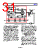
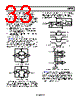
31 / 50 page  Data Sheet AD9739 Rev. E | Page 31 of 50 FINE DELAY DDR FF DBx[13:1] DATA RECEIVER CONTROLLER DCI DELAY SAMPLE DELAY DCI PRE POST SAMPLE DCI WINDOW PRE DCI WINDOW POST DCI WINDOW SAMPLE DATA TO CORE DELAY DELAY FINE DELAY FINE DELAY STATE MACHINE/ TRACKING LOOP ELASTIC FIFO DDR FF DDR FF DDR FF DDR FF 180 0 FDAC DIV-BY-4 TO SYNC CONTROLLER PHASE ROTATION FROM SYNC CONTROLLER OR SPI REG 0x14, BIT[7:6] 90 270 DELAY DELAY DDR FF DDR FF DCI DELAY PATH SAMPLE DELAY PATH DCO DIV-BY-4 Figure 42. Top Level Diagram of the Data Receiver Controller The divide-by-4 circuit generates four clock phases that serve as inputs to the data receiver controller. All of the DDR registers in the data and DCI paths operate on both clock edges; however, for clarity purposes, only the phases (that is, 0 o and 90o) corresponding to the positive edge of each path are shown. One of the divide-by-4 phases is used to generate the DCO signal; therefore, the phase relationship between DCO and clocks fed into the controller remains fixed. Note that it is this attribute that allows possible factory calibration of images and clock spurs attributed to f DAC/4 modulation of the critical DAC clock. Once this data has been successively sampled into the first set of registers, an elastic FIFO is used to transfer the data into the AD9739 clock domain. To continuously track any phase variation between the two clock domains, the data receiver controller should always be enabled and placed into track mode (Register 0x10, Bit 1 and Bit 0). Tracking mode operates continuously in the background to track delay variations between the host and AD9739 clock domains. It does so by ensuring that the DCI signal is sampled within a very narrow window defined by two internally generated clocks (that is, PRE and PST), as shown in Figure 43. Proper sampling of the DCI signal can also be confirmed by monitoring the status of DCI_PRE_PH0 (Register 0x0C, Bit 2) and DCI_PST_PH0 (Register 0x0C, Bit 0). If the delay settings are correct, the state of DCI_ PRE_PH0 should be 0, and the state of DCI_PST_PH0 should be 1. Note that the states of these status bits may toggle occasionally due to cycle-to cycle jitter exceeding the window width. However, the controller averages these status bits over multiple clock cycles to ensure that the DCI signal falls within a programmable window. DCI FINE DELAY PST FINE DELAY PRE FINE_DEL_SKEW Figure 43. Pre- and Post-Delay Sampling Diagram The skew or window width (FINE_DEL_SKEW) is set via Register 0x13, Bits[3:0], with a maximum skew of approximately 180 ps and resolution of 12 ps. It is recommended that the skew be set to 36 ps (that is, Register 0x13 = 0x72) during initialization. The skew setting also affects the speed of the controller loop, with tighter skew settings corresponding to longer response time. Data Receiver Controller Initialization Description The data controller should be initialized and placed into track mode as the second step in the SPI boot sequence. The following steps are recommended for the initialization of the data receiver controller: |
|
链接网址 |
| ALLDATASHEET是否为您带来帮助? [ DONATE ] |
关于 Alldatasheet | 广告服务 | 联系我们 | 隐私政策 | 数据表链接 | 链接交换 | 制造商名单 All Rights Reserved©Alldatasheet.com |
| Russian : Alldatasheetru.com | Korean : Alldatasheet.co.kr | Spanish : Alldatasheet.es | French : Alldatasheet.fr | Italian : Alldatasheetit.com Portuguese : Alldatasheetpt.com | Polish : Alldatasheet.pl | Vietnamese : Alldatasheet.vn Indian : Alldatasheet.in | Mexican : Alldatasheet.com.mx | British : Alldatasheet.co.uk | New Zealand : Alldatasheet.co.nz |
|
Family Site : ic2ic.com |
icmetro.com |
 Chinese ▼
 English
 Chinese
 German
 Japanese
 Russian
 Korean
 Spanish
 French
 Italian
 Portuguese
 Polish
 Vietnamese
 Indian
 Mexican
 British
 New Zealand