|
数据搜索系统,热门电子元器件搜索 |
|
|
数据搜索系统,热门电子元器件搜索 |
|
AD9739-R2-EBZ 数据表(PDF) 33 Page - Analog Devices |
|
|
|||||||||||||||||||||||||||||
AD9739-R2-EBZ 数据表(HTML) 33 Page - Analog Devices |
|
|
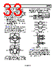
33 / 50 page  Data Sheet AD9739 Rev. E | Page 33 of 50 increase the effective range of the delay line to ensure a DCI_DEL value that falls within a reasonable guard band. In some situations, rotating the phase alone may not be sufficient to create the conditions necessary for the data receiver to lock. This is likely due to a particular misalignment of clock edges within the device that can occur after power up or reset at clock rates below 1.6 GHz. In these situations, it is necessary to power down the device by taking the following steps: 1. Set the four power-down bits in Register 0x01 (Register 0x01 = 0x33). 2. Reset the power-down bits to 0 (Register 0x01 = 0x00) 3. Follow the start-up sequence, including possible phase rotation, as described previously. 4. These three steps may need to be initiated multiple times to achieve a successful lock. LVDS Driver and Receiver Input The AD9739 features a LVDS-compatible driver and receivers. The LVDS driver output used for the DCO and SYNC_OUT signal includes an equivalent 200 Ω source resistor that limits its nominal output voltage swing to ±200 mV when driving a 100 Ω load. The DCO output driver can be powered down via Register 0x01, Bit 5. An equivalent circuit is shown in Figure 44. DCO_N VSS VDD33 DCO_P V+ V+ V– V– 100 Ω VCM 100 Ω ESD ESD Figure 44. Equivalent LVDS Output VSS VDD33 DCI_P DBx[13:0]P DCI_N DBx[13:0]N 100 Ω ESD ESD Figure 45. Equivalent LVDS Input The LVDS receivers include 100 Ω termination resistors, as shown in Figure 45. These receivers meet the IEEE-1596.3-1996 reduced swing specification (with the exception of input hysteresis, which cannot be guaranteed over all process corners). Figure 46 and Figure 47 show an example of nominal LVDS voltage levels seen at the input of the differential receiver with resulting common- mode voltage and equivalent logic level. The LVDS receivers can be powered down via Register 0x01, Bit 4. LVDS INPUTS (NO FAIL-SAFE) VP VP VP VN VN VN LVDS RECEIVER GND 100 Ω VP,N VCOM = (VP + VN)/2 LOGIC BIT EQUIVALENT EXAMPLE 1.4V 1.0V 0.4V –0.4V 0V LOGIC 1 LOGIC 0 Figure 46. LVDS Data Input Levels 100 Ω 100 Ω 100 Ω VDD33 = 3.3V LVDS_1 LVDS_N LVDS_2 VP = 1.4V R1 R2 VP = 1.4V R1 = 4.75 × 100/N R2 = 2.50 × 100/N Figure 47. Resistor Network to Bias Unused LVDS Data Inputs The AD9739 LVDS inputs do not include fail-safe capability. Any unused data input pins should be biased with an external network or static driver. Figure 47 shows an external biasing network that can be used to place unused data bits into a known state. The resistor values for R1 and R2 are selected to establish a VP and VN of 1.4 V and 1.0 V, respectively, depending on the number of unused digital inputs, N. |
|
链接网址 |
| ALLDATASHEET是否为您带来帮助? [ DONATE ] |
关于 Alldatasheet | 广告服务 | 联系我们 | 隐私政策 | 数据表链接 | 链接交换 | 制造商名单 All Rights Reserved©Alldatasheet.com |
| Russian : Alldatasheetru.com | Korean : Alldatasheet.co.kr | Spanish : Alldatasheet.es | French : Alldatasheet.fr | Italian : Alldatasheetit.com Portuguese : Alldatasheetpt.com | Polish : Alldatasheet.pl | Vietnamese : Alldatasheet.vn Indian : Alldatasheet.in | Mexican : Alldatasheet.com.mx | British : Alldatasheet.co.uk | New Zealand : Alldatasheet.co.nz |
|
Family Site : ic2ic.com |
icmetro.com |
 Chinese ▼
 English
 Chinese
 German
 Japanese
 Russian
 Korean
 Spanish
 French
 Italian
 Portuguese
 Polish
 Vietnamese
 Indian
 Mexican
 British
 New Zealand