|
数据搜索系统,热门电子元器件搜索 |
|
|
数据搜索系统,热门电子元器件搜索 |
|
AD9739-R2-EBZ 数据表(PDF) 25 Page - Analog Devices |
|
|
|||||||||||||||||||||||||||||
AD9739-R2-EBZ 数据表(HTML) 25 Page - Analog Devices |
|
|
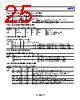
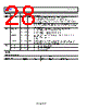
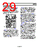
25 / 50 page  Data Sheet AD9739 Rev. E | Page 25 of 50 TxDAC FULL-SCALE CURRENT SETTING (I OUTFS) AND SLEEP Table 14. TxDAC Full-Scale Current Setting (I OUTFS) and Sleep Register Address (Hex) Name Bit R/W Default Setting Comments 0x06 FSC_1 [7:0] R/W 0x00 Sets the TxDAC I OUTFS current between 8 mA and 31 mA (default = 20 mA). I OUTFS = 0.0226 × FSC[9:0] + 8.58, where FSC = 0 to 1023. 0x07 FSC_2 [1:0] R/W 0x02 Sleep 7 R/W 0 = enable DAC output, 1 = disable DAC output (sleep). TxDAC QUAD-SWITCH MODE OF OPERATION Table 15. TxDAC Quad-Switch Mode of Operation Register Address (Hex) Name Bit R/W Default Setting Comments 0x08 DAC-DEC [1:0] R/W 0x00 0x00 = normal baseband mode. 0x01 = return-to-zero mode. 0x02 = mix mode. DCI PHASE ALIGNMENT STATUS Table 16. DCI Phase Alignment Status Register Address (Hex) Name Bit R/W Default Setting Comments 0x0C DCI_PRE_PH0 2 R 0 0 = DCI rising edge is after the PRE delayed version of the Phase 0 sampling edge. 1 = DCI rising edge is before the PRE delayed version of the Phase 0 sampling edge. DCI_PST_PH0 0 R 0 0 = DCI rising edge is after the POST delayed version of the Phase 0 sampling edge. 1 = DCI rising edge is before the POST delayed version of the Phase 0 sampling edge. SYNC_IN PHASE ALIGNMENT STATUS Table 17. SYNC_IN Phase Alignment Status Register Address (Hex) Name Bit R/W Default Setting Comments 0x0D SYNC_IN_PH90 5 R 0 0 = SYNCIN rising edge is after Phase 90 sampling edge. 1 = SYNCIN rising edge is before Phase 90 sampling edge. SYNC_IN_PH0 4 R 0 0 = SYNCIN rising edge is after Phase 0 sampling edge. 1 = SYNCIN rising edge is before Phase 0 sampling edge. DATA RECEIVER CONTROLLER CONFIGURATION Table 18. Data Receiver Controller Configuration Register Address (Hex) Name Bit R/W Default Setting Comments 0x10 SYNC_FLG_RST 7 W 0 Sync controller flag reset. Write 1 followed by 0 to reset flags. SYNC_LOOP_ON 6 R/W 1 0 = disable, 1 = enable. Enable for master only. When enabled, sync controller generates an IRQ when master falls out of lock and automatically begins search/track routine. SYNC_MST/SLV 5 R/W 0 Sync controller configuration. 0 = slave, 1 = master. SYNC_CNT_ENA 4 R/W 0 Sync controller enable. 0 = disable, 1 = enable RCVR_FLG_RST 2 W 0 Data receiver controller flag reset. Write 1 followed by 0 to reset flags. RCVR_LOOP_ON 1 R/W 1 0 = disable, 1 = enable. When enabled, the data receiver controller generates an IRQ; it falls out of lock and automatically begins a search/track routine. RCVR_CNT_ENA 0 R/W 0 Data receiver controller enabled. 0 = disable, 1 = enable. |
|
链接网址 |
| ALLDATASHEET是否为您带来帮助? [ DONATE ] |
关于 Alldatasheet | 广告服务 | 联系我们 | 隐私政策 | 数据表链接 | 链接交换 | 制造商名单 All Rights Reserved©Alldatasheet.com |
| Russian : Alldatasheetru.com | Korean : Alldatasheet.co.kr | Spanish : Alldatasheet.es | French : Alldatasheet.fr | Italian : Alldatasheetit.com Portuguese : Alldatasheetpt.com | Polish : Alldatasheet.pl | Vietnamese : Alldatasheet.vn Indian : Alldatasheet.in | Mexican : Alldatasheet.com.mx | British : Alldatasheet.co.uk | New Zealand : Alldatasheet.co.nz |
|
Family Site : ic2ic.com |
icmetro.com |
 Chinese ▼
 English
 Chinese
 German
 Japanese
 Russian
 Korean
 Spanish
 French
 Italian
 Portuguese
 Polish
 Vietnamese
 Indian
 Mexican
 British
 New Zealand