|
数据搜索系统,热门电子元器件搜索 |
|
|
数据搜索系统,热门电子元器件搜索 |
|
AD9739-R2-EBZ 数据表(PDF) 49 Page - Analog Devices |
|
|
|||||||||||||||||||||||||||||
AD9739-R2-EBZ 数据表(HTML) 49 Page - Analog Devices |
|
|
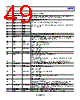
49 / 50 page  Data Sheet AD9739 Rev. E | Page 49 of 50 Table 32. Recommended SPI Initialization with SYNC Controller Enabled Step Address (Hex) Write Value Comments 1 0x00 0x00 Configure for the 4-wire SPI mode with MSB. Note that Bits[7:5] must be mirrored onto Bits[2:0] because the MSB/LSB format can be unknown at power-up. 2 0x00 0x20 Software reset to default SPI values. 3 0x00 0x00 Clear the reset bit. 4 0x22 0x0F Set the common-mode voltage of DACCLK_P and DACCLK_N inputs. 5 0x23 0x0F 6 0x24 0x30 Configure the mu controller. Refer to Table 28 for recommended target mu slope and phase settings vs. clock rate. 7 0x25 0x80 8 0x27 0x44 9 0x28 0x6C 10 0x29 0xCB 11 0x26 0x02 12 0x26 0x03 Enable the mu controller search and track mode. 13 Not applicable Not applicable Wait for 160k × 1/fDATA cycles. 14 0x2A Read back Register 0x2A and confirm that it is equal to 0x01 to ensure that the DLL loop is locked. If it is not locked, proceed to Step 10 and repeat. Limit attempts to three before breaking out of the loop and reporting a mu lock failure. 15 0x15 0x42 Configure sync controller. 16 0x10 0x00 Disable sync controller before enabling it. 17 0x10 0x60 or 0x40 Enable sync controller for loop and IRQ. 0x60 = master mode. 0x40 = slave mode. 18 0x10 0x70 or 0x50 Enable sync controller: 0x70 = master mode. 0x50 = slave mode. 19 Not applicable Not applicable Wait for 160k × 1/fDATA for DLL to lock. 20 0x21 Read back Register 0x21 to confirm proper operation: 0x90 = master mode. 0x00 = slave mode. If not, proceed to Step 15 and repeat. Limit to three attempts before breaking out of loop and reporting sync lock failure. 21 0x0D Read back Register 0x0D and confirm Bits[5:4] = 10. If not, proceed to Step 2 and repeat. Limit to three attempts before breaking out of loop and reporting sync lock failure. 22 Not applicable Not applicable Ensure that the AD9739 is fed with DCI clock input from the data source. 23 0x13 0x72 Set FINE_DEL_SKEW to 2. 24 0x10 0x70 or 0x50 Disable the data Rx controller before enabling it. 0x70 = master mode. 0x50 = slave mode. 25 0x10 0x72 or 0x52 Enable the data Rx controller for loop and IRQ. 0x72 = master mode. 0x52 = slave mode. 26 0x10 0x73 or 0x53 Enable the data Rx controller for search and track mode. 0x73 = master mode. 0x53 = slave mode. 27 Wait for 135k × 1/fDATA cycles. 28 0x21 Read back Register 0x21 and confirm that it is equal to 0x09 to ensure that the DLL loop is locked and tracking. If it is not locked and tracking, proceed to Step 16 and repeat. Limit attempts to three before breaking out of the loop and reporting an Rx data lock failure. 29 Not applicable Not applicable Readback DCI_DEL value in Register 0x13 and Register 0x14 for master and slave. If slave devices are not within 40 codes of each other, re-specify target DCI_DEL value to be average between master and readback DCI_DEL value. 30 0x06, 0x07 0x00, 0x02 Optional: modify the TxDAC IOUTFS setting (the default is 20 mA). 31 0x08 0x00 Optional: modify the TxDAC operation mode (the default is normal mode). |
|
链接网址 |
| ALLDATASHEET是否为您带来帮助? [ DONATE ] |
关于 Alldatasheet | 广告服务 | 联系我们 | 隐私政策 | 数据表链接 | 链接交换 | 制造商名单 All Rights Reserved©Alldatasheet.com |
| Russian : Alldatasheetru.com | Korean : Alldatasheet.co.kr | Spanish : Alldatasheet.es | French : Alldatasheet.fr | Italian : Alldatasheetit.com Portuguese : Alldatasheetpt.com | Polish : Alldatasheet.pl | Vietnamese : Alldatasheet.vn Indian : Alldatasheet.in | Mexican : Alldatasheet.com.mx | British : Alldatasheet.co.uk | New Zealand : Alldatasheet.co.nz |
|
Family Site : ic2ic.com |
icmetro.com |
 Chinese ▼
 English
 Chinese
 German
 Japanese
 Russian
 Korean
 Spanish
 French
 Italian
 Portuguese
 Polish
 Vietnamese
 Indian
 Mexican
 British
 New Zealand