|
数据搜索系统,热门电子元器件搜索 |
|
|
数据搜索系统,热门电子元器件搜索 |
|
AD9739-R2-EBZ 数据表(PDF) 35 Page - Analog Devices |
|
|
|||||||||||||||||||||||||||||
AD9739-R2-EBZ 数据表(HTML) 35 Page - Analog Devices |
|
|
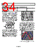
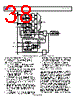
35 / 50 page  Data Sheet AD9739 Rev. E | Page 35 of 50 The mu phase characteristics can vary significantly among devices due to gm variations in the digital delay line that are sensitive to process skews (along with temperature and supply). As a result, careful selection of the target phase location is required such that the mu controller can converge upon this phase location for all devices. Figure 50 shows that mu phase characteristics of three devices at 25°C from slow, nominal, and fast skew lots at 1.2 GSPS. Note that a −6 mu phase setting does not map to any delay line tap setting for the fast process skew case; therefore, another target mu phase is recommended at this clock rate. Table 28 provides a list of recommended mu phase/slope settings over the specified clock range of the AD9739 based on the considerations previously described. These values should be used to ensure robust operation of the mu controller. Table 28. Recommended Target Mu Phase Settings vs. Clock Rate Clock Rate (GSPS) Slope Mu Phase 0.8 − 6 0.9 − 4 1.0 + 5 1.1 + 8 1.2 + 12 1.3 − 12 1.4 − 10 1.5 − 8 1.6 to 2.5 − 6 After the mu controller completes its search and establishes lock on the target mu phase, it attempts to maintain a constant timing relationship between the two clock domains over the specified temperature and supply range. If the mu controller requests a mu delay setting that exceeds the tapped delay line range (that is, <0 or >432), the mu controller can lose lock, causing possible system disruption (that is, can generate IRQ or restart the search). To avoid this scenario, symmetrical guard bands are recommended at each end of the mu delay range. The guard band scaling is such that one LSB of Guard[4:0] (Register 0x29) corresponds to eight LSBs of MUDEL (Register 0x28). The recommended guard band setting of 11 (that is, Register 0x29 = 0xCB) corresponds to 88 LSBs, thus providing sufficient margin. Mu Controller Initialization Description The mu controller must be initialized and placed into track mode as a first step in the SPI boot sequence. The following steps are required for initialization of the mu controller. Note that the AD9739 data sheet specifications and characterization data are based on the following mu controller settings: 1. Turn on the phase detector with boost (Register 0x24 = 0x30). 2. Enable the mu delay controller duty-cycle correction circuitry and specify the recommended slope for phase. (that is, Register 0x25 = 0x80 corresponds to a negative slope). 3. Specify search/track mode with a recommended target phase, SET_PHS, of 6 (for example) and an initial MUDEL[8:0] setting of 216 (Register 0x27 = 0x46 and Register 0x28 = 0x6C). 4. Set search tolerance to exact and retry if the search fails its initial attempt. Also, set the guard band to the recommended setting of 11 (Register 0x29 = 0xCB). 5. Set the mu controller tracking gain to the recommended setting and enable the mu controller state machine (Register 0x26 = 0x03). Upon completion of the last step, the mu controller begins a search algorithm that starts with an initial delay setting specified by the MUDEL register (that is, 216, which corresponds to the midpoint of the delay line). The initial search algorithm works by sweeping through different mu delay values in an alternating manner until the desired phase (that is, a SET_PHS of 4) is exactly measured. When the desired phase is measured, the slope of the phase measurement is then calculated and compared against the specified slope (slope = negative). If everything matches, the search algorithm is finished. If not, the search continues in both directions until an exact match can be found or a programmable guard band is reached in one of the directions. When the guard band is reached, the search still continues but only in the opposite direction. If the desired phase is not found before the guard band is reached in the second direction, the search changes back to the alternating mode and continues looking within the guard band. The typical locking time for the mu controller is approximately 180k DAC cycles (at 2 GSPS ~ 75 µs). The search fails if the mu delay controller reaches the endpoints. The mu controller can be configured to retry (Register 0x29, Bit 6) the search or stop. For applications that have a microcontroller, the preferred approach is to poll the MU_LKD status bit (Register 0x2A, Bit 0) after the typical locking time has expired. This method allows the system controller to check the status of other system parameters (that is, power supplies and clock source) before reattempting the search (by writing 0x03 to Register 0x26). For applications that do not have polling capabilities, the mu controller state machine should be reconfigured to restart the search in hopes that the system’s condition that did not cause locking on the first attempt has disappeared. Once the mu delay value is found that exactly matches the desired mu phase setting and slope (for example, 6 with a negative. slope), the mu controller goes into track mode. In this mode, the mu controller makes slight adjustments to the delay value to track any variations between the two clock paths due to temperature, time, and supply variations. Two status bits, MU_LKD (Register 0x2A, Bit 0) and MU_LST (Register 0x2A, Bit 1) are available to the user to signal the existing status control loop. If the current phase is more than four steps away from the desired phase, the MU_LKD bit is cleared, and if the lock acquired was previously set, the MU_LST bit is set. Should the phase deviation return to within three steps, the MU_LKD bit is set again while the MU_LST is cleared. Note that this sort of event may occur if the main clock input (that is, DACCLK) is disrupted or the mu controller exceeds the tapped delay line range (that is, <0 or >432). |
|
链接网址 |
| ALLDATASHEET是否为您带来帮助? [ DONATE ] |
关于 Alldatasheet | 广告服务 | 联系我们 | 隐私政策 | 数据表链接 | 链接交换 | 制造商名单 All Rights Reserved©Alldatasheet.com |
| Russian : Alldatasheetru.com | Korean : Alldatasheet.co.kr | Spanish : Alldatasheet.es | French : Alldatasheet.fr | Italian : Alldatasheetit.com Portuguese : Alldatasheetpt.com | Polish : Alldatasheet.pl | Vietnamese : Alldatasheet.vn Indian : Alldatasheet.in | Mexican : Alldatasheet.com.mx | British : Alldatasheet.co.uk | New Zealand : Alldatasheet.co.nz |
|
Family Site : ic2ic.com |
icmetro.com |
 Chinese ▼
 English
 Chinese
 German
 Japanese
 Russian
 Korean
 Spanish
 French
 Italian
 Portuguese
 Polish
 Vietnamese
 Indian
 Mexican
 British
 New Zealand