|
数据搜索系统,热门电子元器件搜索 |
|
|
数据搜索系统,热门电子元器件搜索 |
|
AD9739-R2-EBZ 数据表(PDF) 38 Page - Analog Devices |
|
|
|||||||||||||||||||||||||||||
AD9739-R2-EBZ 数据表(HTML) 38 Page - Analog Devices |
|
|
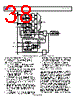
38 / 50 page  AD9739 Data Sheet Rev. E | Page 38 of 50 90 0 DB0[13:0] DB1[13:0] DCI DB0 EVEN DB0 ODD DB1 EVEN DB1 ODD DCO fDAC/4 SYNC_IN SYNC_OUT DIV-BY-4 0/180 RX DATA CONTROLLER 90/270 STATE MACHINE TRACKING LOOP PHASE ROTATOR SLAVE ONLY TO DAC DELAY DELAY fDAC Mu Delay MU DELAY fDAC DISTRIBUTION SYNCHRONIZATION CONTROLLER 0 180 270 90 DIV-BY-4 DELAY STATE MACHINE TRACKING LOOP PHASE COMPARISON Figure 53. Top Level Block Diagram of Synchronization Circuitry and Controller Figure 53 shows a top-level diagram of the synchronization controller (bottom) and how it interfaces to other digital functional blocks within the AD9739. Note the following observations of this top level diagram: • Synchronization between multiple devices is achieved by rotating the divide-by-4 phases of the slave devices such that they align with the master. • For the slave devices, the sync controller compares the phase alignment of the master’s SYNC_IN reference signal with the initial 0 o/90o outputs of the divide-by-4 and then rotates the divide-by-4 phase until the SYNC_IN signal falls between these phases. • A reference signal common to all devices is required for synchronization. The master device generates this signal by providing a SYNC_OUT signal which is then distributed to all the devices (including itself with tight time alignment) as a SYNC_IN signal. • Because the SYNC_IN signal has a defined relationship between the divide-by-4 phase of the master, the slave devices can now align their respective divide-by-4 phases to the SYNC_IN phase thus ensuring phase alignment among all devices. • It is not possible to manually rotate the divide-by-4 phases of the data path with the sync controller enabled. This can be a problem at lower clock rates were one may desire to rotate the divide-by-4 phase to ensure locking of the data receiver controller and/or achieve a more optimum DCI_DEL value. • The DCO output signal is generated from a separate divide-by-4 circuit, and therefore, has a random phase upon each startup. For this reason, the DCO of the master should be distributed to all the FPGAs. SYNC Controller Initialization Description The sync controller of the master is enabled by writing 0x70 to Register 0x10. Once enabled, a state machine automatically adjusts the output delay of its SYNC_OUT signal such that the fed back reference SYNC_IN signal is centered between the 0° and 90° output phases associated with its divide-by-4 circuit. Note that the coarse delay is performed by shifting phases via PHZ MUX while the fine delay that centers (and tracks) variation is done by a variable delay line. The variable delay line tap size is 12 ps. Once SYNC_IN is centered, the controller enters tracking mode such that SYNC_IN remains centered despite possible system variations in temperature and/or supply. Centering the SYNC_IN signal on the master device ensures that the SYNC_IN signals of the slave devices also remain centered between their respective divide-by-4 phases; therefore, providing the greatest margin to absorb nonideal timing skews. The following status bits |
|
链接网址 |
| ALLDATASHEET是否为您带来帮助? [ DONATE ] |
关于 Alldatasheet | 广告服务 | 联系我们 | 隐私政策 | 数据表链接 | 链接交换 | 制造商名单 All Rights Reserved©Alldatasheet.com |
| Russian : Alldatasheetru.com | Korean : Alldatasheet.co.kr | Spanish : Alldatasheet.es | French : Alldatasheet.fr | Italian : Alldatasheetit.com Portuguese : Alldatasheetpt.com | Polish : Alldatasheet.pl | Vietnamese : Alldatasheet.vn Indian : Alldatasheet.in | Mexican : Alldatasheet.com.mx | British : Alldatasheet.co.uk | New Zealand : Alldatasheet.co.nz |
|
Family Site : ic2ic.com |
icmetro.com |
 Chinese ▼
 English
 Chinese
 German
 Japanese
 Russian
 Korean
 Spanish
 French
 Italian
 Portuguese
 Polish
 Vietnamese
 Indian
 Mexican
 British
 New Zealand