|
数据搜索系统,热门电子元器件搜索 |
|
|
数据搜索系统,热门电子元器件搜索 |
|
AD9739-R2-EBZ 数据表(PDF) 39 Page - Analog Devices |
|
|
|||||||||||||||||||||||||||||
AD9739-R2-EBZ 数据表(HTML) 39 Page - Analog Devices |
|
|
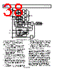
39 / 50 page  Data Sheet AD9739 Rev. E | Page 39 of 50 are available in Register 0x21 indicating lock, lost-lock, and tracking: SYNC_LCK, SYNC_LST and SYNC_TRK_ON. The sync controller of the slave is enabled by writing 0x50 to Register 0x10. Once enabled, the state machine compares the reference SYNC_IN signal to the 0°/90° phase outputs of the divide-by-4 phase settings. If the SYNC_IN signal does not fall between these phases, the state machine of the slave rotates the divide-by-4 phase setting until it does. To validate that phase alignment has been achieved, the SYNC_IN_PH90 and SYNC_IN_PH0 status bits should read 1 and 0, respectively (that is, Register 0x0D, Bits[5:4]). Note that the DCO and SYNC_OUT outputs of the slave can be disabled via Register 0x01, Bit 5. Synchronization Limitations Ensuring consistent synchronization over production lots in systems containing two or more AD9739 devices becomes increasingly more challenging at the higher update rates because the timing offset between adjacent phases of the divide-by-4 output clock is equal to 1/f DAC . For example, a DAC update of 2 GSPS corresponds to a 500 ps period. If the SYNC_IN signal of an ideal master device is positioned in the center of its divide-by-4 0 o and 90 o phase outputs, only ±250 ps of timing margin exists for the slave devices. This ideal margin is actually reduced by quadrature phase errors in the divide-by-4 circuit of the master as well as its ability to position the SYNC_IN exactly in the center of the 0° and 90° output phases. The timing margin is further eroded by the following sources: • Master-to-slave device(s) mismatch in the propagation delays in the mu delay clock path and SYNC_IN. Note that these mismatches can be up to 100 ps between devices that are at opposite extremes of the process corners. • Quadrature phase errors in the divide-by-4 outputs of the slave. These sources of timing skews become more significant as the DACCLK period is decreased (that is, clock rate is increased), leaving less margin for timing skews external to the master-to- slave device(s). Special consideration to PCB layout and selection of clock distribution ICs are required to ensure minimum skew between the distributed DACCLK and SYNC_IN signals. Note that timing skews can quickly accumulate considering that the propagation delay on an FR4 PCB is on the order of 170 ps/inch, and that output-to-output skews on each clock distribution IC can be as high as 25 ps. The problem becomes more pronounced in multiboard synchronization where clock signals (that is, DACCLK, SYNC_OUT, and DCO) are distributed over a back plane to multiple PCBs. Data alignment among the various data sources is required when driven by phase aligned DCO signals that are a buffered version of the master’s DCO. However, these data sources (FPGAs) also have process, supply voltage, and temperature sensitivities (PVTs) that can cause misalignment among their respective DCI outputs. Adding to this dilemma is that it also possible for the data receiver controller of different AD9739 devices to converge on different delay settings due to PVT variations of the delay line (even if DCI inputs are exactly aligned). This can result in a four sample pipeline mismatch between devices if the difference in absolute delays exceeds a period of 4/f DAC. Recall that the controller searches up/down for its first valid edge from its initial start value (that is, DCI_DEL and SMP_DEL). While the initial start values between devices should be made the same, different absolute time delays due to PVT can cause devices to converge on different edges of DCI above or below this initial start value. As a result, confirm that DCI_DEL values between multiple devices are matched sufficiently such that the absolute differences between the readback DCI_DEL values do not exceed a data period (that is, 4/f DAC). If the difference exceeds a data period, modify the DCI_DEL (and SMP_DEL) setting of the slave device so that its start point is roughly ½ the difference between the master and slave readback values. |
|
链接网址 |
| ALLDATASHEET是否为您带来帮助? [ DONATE ] |
关于 Alldatasheet | 广告服务 | 联系我们 | 隐私政策 | 数据表链接 | 链接交换 | 制造商名单 All Rights Reserved©Alldatasheet.com |
| Russian : Alldatasheetru.com | Korean : Alldatasheet.co.kr | Spanish : Alldatasheet.es | French : Alldatasheet.fr | Italian : Alldatasheetit.com Portuguese : Alldatasheetpt.com | Polish : Alldatasheet.pl | Vietnamese : Alldatasheet.vn Indian : Alldatasheet.in | Mexican : Alldatasheet.com.mx | British : Alldatasheet.co.uk | New Zealand : Alldatasheet.co.nz |
|
Family Site : ic2ic.com |
icmetro.com |
 Chinese ▼
 English
 Chinese
 German
 Japanese
 Russian
 Korean
 Spanish
 French
 Italian
 Portuguese
 Polish
 Vietnamese
 Indian
 Mexican
 British
 New Zealand