|
数据搜索系统,热门电子元器件搜索 |
|
|
数据搜索系统,热门电子元器件搜索 |
|
EM357-RTR 数据表(PDF) 135 Page - List of Unclassifed Manufacturers |
|
|
|||||||||||||||||||||||||||||
EM357-RTR 数据表(HTML) 135 Page - List of Unclassifed Manufacturers |
|
|
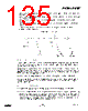
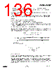
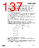
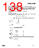
135 / 240 page  EM351 / EM357 Select the active input for TIMx_CCR2by writing the TIM_CC2S bits to 10 in the TIMx_CCMR1 register (TI1 selected). Select the active polarity for TI1FP2 (used for capture in the TIMx_CCR2) by writing the TIM_CC2P bit to 1 (active on falling edge). Select the valid trigger input by writing the TIM_TS bits to 101 in the TIMx_SMCR register (TI1FP1 selected). Configure the slave mode controller in reset mode by writing the TIM_SMS bits to 100 in the TIMx_SMCR register. Enable the captures by writing the TIM_CC1E and TIM_CC2E bits to 1 in the TIMx_CCER register. Figure 9-20 illustrates this example. Figure 9-20. PWM Input Mode Timing 9.3.7 Forced Output Mode In output mode (CCyS bits = 00 in the TIMx_CCMR1 register), software can force each output compare signal (OCyREF and then OCy) to an active or inactive level independently of any comparison between the output compare register and the counter. To force an output compare signal (OCyREF/OCy) to its active level, write 101 in the TIM_OCyM bits in the corresponding TIMx_CCMR1 register. OCyREF is forced high (OCyREF is always active high) and OCy gets the opposite value to the TIM_CCyP polarity bit. For example, TIM_CCyP = 0 defines OCy as active high, so when OCyREF is active, OCy is also set to a high level. The OCyREF signal can be forced low by writing the TIM_OCyM bits to 100 in the TIMx_CCMR1 register. The comparison between the TIMx_CCRy shadow register and the counter is still performed and allows the INT_TIMxCCRyIF flag to be set. Interrupt requests can be sent accordingly. This is described in the output compare mode section. 9.3.8 Output Compare Mode This mode is used to control an output waveform or to indicate when a period of time has elapsed. When a match is found between the capture/compare register and the counter, the output compare function: Assigns the corresponding output pin to a programmable value defined by the output compare mode (the TIM_OCyM bits in the TIMx_CCMR1 register) and the output polarity (the TIM_CCyP bit in the TIMx_CCER register). The output can be frozen (TIM_OCyM = 000), be set active (TIM_OCyM = 001), be set inactive (TIM_OCyM = 010), or can toggle (TIM_OCyM = 011) on the match. 9-15 120-035X-000D Preliminary |
|
链接网址 |
| ALLDATASHEET是否为您带来帮助? [ DONATE ] |
关于 Alldatasheet | 广告服务 | 联系我们 | 隐私政策 | 数据表链接 | 链接交换 | 制造商名单 All Rights Reserved©Alldatasheet.com |
| Russian : Alldatasheetru.com | Korean : Alldatasheet.co.kr | Spanish : Alldatasheet.es | French : Alldatasheet.fr | Italian : Alldatasheetit.com Portuguese : Alldatasheetpt.com | Polish : Alldatasheet.pl | Vietnamese : Alldatasheet.vn Indian : Alldatasheet.in | Mexican : Alldatasheet.com.mx | British : Alldatasheet.co.uk | New Zealand : Alldatasheet.co.nz |
|
Family Site : ic2ic.com |
icmetro.com |
 Chinese ▼
 English
 Chinese
 German
 Japanese
 Russian
 Korean
 Spanish
 French
 Italian
 Portuguese
 Polish
 Vietnamese
 Indian
 Mexican
 British
 New Zealand