|
数据搜索系统,热门电子元器件搜索 |
|
|
数据搜索系统,热门电子元器件搜索 |
|
EM357-RTR 数据表(PDF) 180 Page - List of Unclassifed Manufacturers |
|
|
|||||||||||||||||||||||||||||
EM357-RTR 数据表(HTML) 180 Page - List of Unclassifed Manufacturers |
|
|
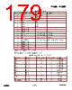
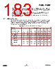
180 / 240 page  EM351 / EM357 10.1.5.2 Input Range ADC inputs can be routed through input buffers to expand the input voltage range. The input buffers have a fixed 0.25 gain and the converted data is scaled by that factor. With the input buffers disabled the single-ended input range is 0 V to VREF and the differential input range is -VREF to +VREF. With the input buffers enabled the single-ended range is within 100 mV of the supply range limits: 0 V to VDD_PADS single-ended and -VDD_PADS to +VDD_PADS differential. The input buffers are enabled for the ADC P and N inputs by setting the ADC_HVSELP and ADC_HVSELN bits respectively, in the ADC_CFG register. The ADC accuracy is reduced when the input buffer is selected. 10.1.5.3 Sample Time ADC sample time is programmed by selecting the sampling clock and the clocks per sample. The sampling clock may be either 1 MHz or 6 MHz. If the ADC_1MHZCLK bit in the ADC_CFG register is clear, the 6 MHz clock is used; if it is set, the 1 MHz clock is selected. The 6 MHz sample clock offers faster conversion times but the ADC resolution is lower than that achieved with the 1 MHz clock. The number of clocks per sample is determined by the ADC_PERIOD bits in the ADC_CFG register. ADC_PERIOD values select from 32 to 4096 sampling clocks in powers of two. Longer sample times produce more significant bits. Regardless of the sample time, converted samples are always 16-bits in size with the significant bits left-aligned within the value. Table 10-4 shows the options for ADC sample times and the significant bits in the conversion results. Table 10-4. ADC Sample Times Sample Time (µs) Sample Frequency (kHz) ADC_PERIOD Sample Clocks 1 MHz clock 6 MHz clock 1 MHz clock 6 MHz clock Significant Bits 0 32 32 5.33 31.3 188 7 1 64 64 10.7 15.6 93.8 8 2 128 128 21.3 7.81 46.9 9 3 256 256 42.7 3.91 23.4 10 4 512 512 85.3 1.95 11.7 11 5 1024 1024 170 0.977 5.86 12 6 2048 2048 341 0.488 2.93 13 7 4096 4096 682 0.244 1.47 14 Note: ADC sample timing is the same whether the EM35x is using the 24 MHz crystal oscillator or the 12 MHz high-speed RC oscillator. This facilitates using the ADC soon after the CPU wakes from deep sleep, before switching to the crystal oscillator. 10.2 Interrupts The ADC has its own top-level interrupt in the NVIC. The ADC interrupt is enabled by writing the INT_ADC bit to the INT_CFGSET register, and cleared by writing the INT_ADC bit to the INT_CFGCLR register. Chapter11, Interrupt System, describes the interrupt system in detail. 10-5 120-035X-000D Preliminary |
|
链接网址 |
| ALLDATASHEET是否为您带来帮助? [ DONATE ] |
关于 Alldatasheet | 广告服务 | 联系我们 | 隐私政策 | 数据表链接 | 链接交换 | 制造商名单 All Rights Reserved©Alldatasheet.com |
| Russian : Alldatasheetru.com | Korean : Alldatasheet.co.kr | Spanish : Alldatasheet.es | French : Alldatasheet.fr | Italian : Alldatasheetit.com Portuguese : Alldatasheetpt.com | Polish : Alldatasheet.pl | Vietnamese : Alldatasheet.vn Indian : Alldatasheet.in | Mexican : Alldatasheet.com.mx | British : Alldatasheet.co.uk | New Zealand : Alldatasheet.co.nz |
|
Family Site : ic2ic.com |
icmetro.com |
 Chinese ▼
 English
 Chinese
 German
 Japanese
 Russian
 Korean
 Spanish
 French
 Italian
 Portuguese
 Polish
 Vietnamese
 Indian
 Mexican
 British
 New Zealand