|
数据搜索系统,热门电子元器件搜索 |
|
|
数据搜索系统,热门电子元器件搜索 |
|
TDA4VEN...Q1 数据表(PDF) 87 Page - Texas Instruments |
|
|
|||||||||||||||||||||||||||||
TDA4VEN...Q1 数据表(HTML) 87 Page - Texas Instruments |
|
|
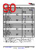
87 / 236 page  6.6 Electrical Characteristics Note The interfaces or signals described in Section 6.6 correspond to the interfaces or signals available in multiplexing mode 0 (Primary Signal Function). All interfaces or signals multiplexed on the balls described in these tables have the same DC electrical characteristics, unless multiplexing involves a PHY and GPIO combination, in which case different DC electrical characteristics are specified for the different multiplexing modes (Functions). 6.6.1 I2C Open-Drain, and Fail-Safe (I2C OD FS) Electrical Characteristics over recommended operating conditions (unless otherwise noted) PARAMETER TEST CONDITIONS MIN TYP MAX UNIT 1.8V MODE VIL Input Low Voltage 0.3 × VDD (1) V VILSS Input Low Voltage Steady State 0.3 × VDD (1) V VIH Input High Voltage 0.7 × VDD (1) 1.98(2) V VIHSS Input High Voltage Steady State 0.7 × VDD (1) V VHYS Input Hysteresis Voltage 0.1 × VDD (1) mV IIN Input Leakage Current. VI = 1.8V or VI = 0V ±10 µA VOL Output Low Voltage 0.2 × VDD (1) V IOL (3) Low Level Output Current VOL(MAX) 10 mA SRI (5) Input Slew Rate 18f(4) or 1.8E+6 V/s 3.3V MODE (6) VIL Input Low Voltage 0.3 × VDD (1) V VILSS Input Low Voltage Steady State 0.25 × VDD (1) V VIH Input High Voltage 0.7 × VDD (1) 3.63(2) V VIHSS Input High Voltage Steady State 0.7 × VDD (1) V VHYS Input Hysteresis Voltage 0.05 × VDD (1) mV IIN Input Leakage Current. VI = 3.3V or VI = 0V ±10 µA VOL Output Low Voltage 0.4 V IOL (3) Low Level Output Current VOL(MAX) 10 mA SRI (5) Input Slew Rate 33f(4) or 3.3E+6 8E+7 V/s (1) VDD stands for corresponding power supply. For more information on the power supply name and the corresponding ball(s), see POWER column of the Pin Attributes table. (2) This value also defines the Absolute Maximum Ratings value the IO. (3) The IOL parameter defines the minimum Low Level Output Current for which the device is able to maintain the specified VOL value. The value defined by this parameter should be considered the maximum current available to a system implementation which needs to maintain the specified VOL value for attached components. (4) f = toggle frequency of the input signal in Hz. (5) This MIN parameter only applies to input signal functions which are not defined in their respective Timing and Switching Characteristics sections. Select the MIN parameter which results in the largest value. (6) I2C Hs-mode is not supported when operating the IO in 3.3V mode. www.ti.com TDA4VEN-Q1, TDA4AEN-Q1 SPRSP96A – MARCH 2024 – REVISED SEPTEMBER 2024 Copyright © 2024 Texas Instruments Incorporated Submit Document Feedback 87 Product Folder Links: TDA4VEN-Q1 TDA4AEN-Q1 |
|
链接网址 |
| ALLDATASHEET是否为您带来帮助? [ DONATE ] |
关于 Alldatasheet | 广告服务 | 联系我们 | 隐私政策 | 数据表链接 | 链接交换 | 制造商名单 All Rights Reserved©Alldatasheet.com |
| Russian : Alldatasheetru.com | Korean : Alldatasheet.co.kr | Spanish : Alldatasheet.es | French : Alldatasheet.fr | Italian : Alldatasheetit.com Portuguese : Alldatasheetpt.com | Polish : Alldatasheet.pl | Vietnamese : Alldatasheet.vn Indian : Alldatasheet.in | Mexican : Alldatasheet.com.mx | British : Alldatasheet.co.uk | New Zealand : Alldatasheet.co.nz |
|
Family Site : ic2ic.com |
icmetro.com |
 Chinese ▼
 English
 Chinese
 German
 Japanese
 Russian
 Korean
 Spanish
 French
 Italian
 Portuguese
 Polish
 Vietnamese
 Indian
 Mexican
 British
 New Zealand