|
数据搜索系统,热门电子元器件搜索 |
|
|
数据搜索系统,热门电子元器件搜索 |
|
EM357-RTR 数据表(PDF) 51 Page - Silicon Laboratories |
|
|
|||||||||||||||||||||||||||||
EM357-RTR 数据表(HTML) 51 Page - Silicon Laboratories |
|
|
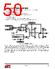
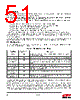
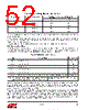
51 / 241 page  51 Rev 1.3 7.1. GPIO Ports The 24 GPIO pins are grouped into three ports: PA, PB, and PC. Individual GPIOs within a port are numbered 0 to 7 according to their bit positions within the GPIO registers. Note: Because GPIO port registers’ functions are identical, the notation Px is used here to refer to PA, PB, or PC. For example, GPIO_PxIN refers to the registers GPIO_PAIN, GPIO_PBIN, and GPIO_PCIN. Each of the three GPIO ports has the following registers whose low-order eight bits correspond to the port’s eight GPIO pins: GPIO_PxIN (input data register) returns the pin level (unless in analog mode). GPIO_PxOUT (output data register) controls the output level in normal output mode. GPIO_PxCLR (clear output data register) clears bits in GPIO_PxOUT. GPIO_PxSET (set output data register) sets bits in GPIO_PxOUT. GPIO_PxWAKE (wake monitor register) specifies the pins that can wake the EM35x. In addition to these registers, each port has a pair of configuration registers, GPIO_PxCFGH and GPIO_PxCFGL. These registers specify the basic operating mode for the port’s pins. GPIO_PxCFGL configures the pins Px[3:0] and GPIO_PxCFGH configures the pins Px[7:4]. For brevity, the notation GPIO_PxCFGH/L refers to the pair of configuration registers. Five GPIO pins (PA6, PA7, PB6, PB7 and PC0) can sink and source higher current than standard GPIO outputs. Refer to Table 2.5 Digital I/O Specifications in "2. Electrical Specifications" on page 8 for more information. 7.2. Configuration Each pin has a 4-bit configuration value in the GPIO_PxCFGH/L register. The various GPIO modes and their 4-bit configuration values are shown in Table 7.1. If a GPIO has two peripherals that can be the source of alternate output mode data, then other registers in addition to GPIO_PxCFGH/L determine which peripheral controls the output. Several GPIOs share an alternate output with Timer 2 and the Serial Controllers. Bits in Timer 2’s TIM2_OR register control routing Timer 2 outputs to different GPIOs. Bits in Timer 2’s TIM2_CCER register enable Timer 2 outputs. When Timer 2 outputs are enabled they override Serial Controller outputs. Table 7.2 indicates the GPIO mapping for Timer 2 outputs depending on the bits in the register TIM2_OR. Refer to "9. General Purpose Timers (TIM1 and TIM2)" on page 114 for complete information on timer configuration. Table 7.1. GPIO Configuration Modes GPIO Mode GPIO_PxCFGH/L Description Analog 0x0 Analog input or output. When in analog mode, the digital input (GPI- O_PxIN) always reads 1. Input (floating) 0x4 Digital input without an internal pull up or pull down. Output is disabled. Input (pull-up or pull-down) 0x8 Digital input with an internal pull up or pull down. A set bit in GPIO_Px- OUT selects pull up and a cleared bit selects pull down. Output is dis- abled. Output (push-pull) 0x1 Push-pull output. GPIO_PxOUT controls the output. Output (open- drain) 0x5 Open-drain output. GPIO_PxOUT controls the output. If a pull up is required, it must be external. Alternate Output (push-pull) 0x9 Push-pull output. An onboard peripheral controls the output. Alternate Output (open-drain) 0xD Open-drain output. An onboard peripheral controls the output. If a pull up is required, it must be external. |
|
链接网址 |
| ALLDATASHEET是否为您带来帮助? [ DONATE ] |
关于 Alldatasheet | 广告服务 | 联系我们 | 隐私政策 | 数据表链接 | 链接交换 | 制造商名单 All Rights Reserved©Alldatasheet.com |
| Russian : Alldatasheetru.com | Korean : Alldatasheet.co.kr | Spanish : Alldatasheet.es | French : Alldatasheet.fr | Italian : Alldatasheetit.com Portuguese : Alldatasheetpt.com | Polish : Alldatasheet.pl | Vietnamese : Alldatasheet.vn Indian : Alldatasheet.in | Mexican : Alldatasheet.com.mx | British : Alldatasheet.co.uk | New Zealand : Alldatasheet.co.nz |
|
Family Site : ic2ic.com |
icmetro.com |
 Chinese ▼
 English
 Chinese
 German
 Japanese
 Russian
 Korean
 Spanish
 French
 Italian
 Portuguese
 Polish
 Vietnamese
 Indian
 Mexican
 British
 New Zealand