|
数据搜索系统,热门电子元器件搜索 |
|
|
数据搜索系统,热门电子元器件搜索 |
|
EM357-RTR 数据表(PDF) 31 Page - Silicon Laboratories |
|
|
|||||||||||||||||||||||||||||
EM357-RTR 数据表(HTML) 31 Page - Silicon Laboratories |
|
|
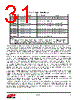
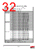
31 / 241 page  Rev 1.3 31 Table 5.2 shows the mapping of the option bytes that are used for read and write protection of the flash. Each bit of the flash write protection option bytes protects a 4 page region of the main flash block. The EM351 has 16 regions and therefore option bytes 4 and 5 control flash write protection (option byte 6 is reserved/unused). The EM357 has 24 regions and therefore option bytes 4, 5, and 6 control flash write protection. These write protection bits are active low, and therefore the erased state of 0xFF disables write protection. Like read protection, write protection only takes effect after a reset. Write protection not only prevents a write to the region, but also prevents page erasure. Option byte 0 controls flash read protection. When option byte 0 is set to 0xA5, read protection is disabled. All other values, including the erased state 0xFF, enable read protection when coming out of reset. The internal state of read protection (active versus disabled) can only be changed by applying a full chip reset. If a debugger is connected to the EM35x, the intrusion state is latched. Read protection is combined with this latched intrusion signal. When both read protection and intrusion are set, all flash is disconnected from the internal bus. As a side effect, the CPU cannot execute code since all flash is disconnected from the bus. This functionality prevents a debug tool from being able to read the contents of any flash. The only means of clearing the intrusion signal is to disconnect the debugger and reset the entire chip using the nRESET pin. By requiring a chip reset, a debugger cannot install or execute malicious code that could allow the contents of the flash to be read. The only way to disable read protection is to program option byte 0 with the value 0xA5. Option byte 0 must be erased before it can be programmed. Erasing option byte 0 while read protection is active automatically mass- erases the main flash block. By automatically erasing main flash, a debugger cannot disable read protection and readout the contents of main flash without destroying its contents. When read protection is active, the bottom four flash pages, addresses 0x08000000 to 0x08001FFF, are automatically write-protected. Write protecting the bottom four flash pages of main flash prevents an attacker from reprogramming the reset vector and executing arbitrary code. In general, if read protection is active then write protection should also be active. This prevents an attacker from reprogramming flash with malicious code that could readout the flash after the debugger is disconnected. Even though read protection automatically protects the reset vector, the same technique of reprogramming flash could be performed at an address outside the bottom four flash pages. To obtain fully protected flash, both read protection and write protection should be active. Table 5.1. Option Byte Storage Address bits [15:8] bits [7:0] Notes 0x08040800 Inverse Option Byte 0 Option Byte 0 Configures flash read protection 0x08040802 Inverse Option Byte 1 Option Byte 1 Reserved 0x08040804 Inverse Option Byte 2 Option Byte 2 Available for customer use1 0x08040806 Inverse Option Byte 3 Option Byte 3 Available for customer use1 0x08040808 Inverse Option Byte 4 Option Byte 4 Configures flash write protection 0x0804080A Inverse Option Byte 5 Option byte 5 Configures flash write protection 0x0804080C Inverse Option Byte 6 Option Byte 6 Configures flash write protection2 0x0804080E Inverse Option Byte 7 Option Byte 7 Reserved Notes: 1. Option bytes 2 and 3 do not link to any specific hardware functionality other than the option byte loader. Therefore, they are best used for storing data that requires a hardware verification of the data integrity. 2. Option byte 6 is reserved/unused in the EM351 due to the smaller flash size. |
|
链接网址 |
| ALLDATASHEET是否为您带来帮助? [ DONATE ] |
关于 Alldatasheet | 广告服务 | 联系我们 | 隐私政策 | 数据表链接 | 链接交换 | 制造商名单 All Rights Reserved©Alldatasheet.com |
| Russian : Alldatasheetru.com | Korean : Alldatasheet.co.kr | Spanish : Alldatasheet.es | French : Alldatasheet.fr | Italian : Alldatasheetit.com Portuguese : Alldatasheetpt.com | Polish : Alldatasheet.pl | Vietnamese : Alldatasheet.vn Indian : Alldatasheet.in | Mexican : Alldatasheet.com.mx | British : Alldatasheet.co.uk | New Zealand : Alldatasheet.co.nz |
|
Family Site : ic2ic.com |
icmetro.com |
 Chinese ▼
 English
 Chinese
 German
 Japanese
 Russian
 Korean
 Spanish
 French
 Italian
 Portuguese
 Polish
 Vietnamese
 Indian
 Mexican
 British
 New Zealand