|
数据搜索系统,热门电子元器件搜索 |
|
|
数据搜索系统,热门电子元器件搜索 |
|
EM357-RTR 数据表(PDF) 33 Page - Silicon Laboratories |
|
|
|||||||||||||||||||||||||||||
EM357-RTR 数据表(HTML) 33 Page - Silicon Laboratories |
|
|
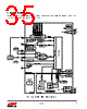
33 / 241 page  Rev 1.3 33 5.2.1.5. Simulated EEPROM Ember software reserves 8 kB of the main flash block as a simulated EEPROM storage area for stack and customer tokens. The simulated EEPROM storage area implements a wear-leveling algorithm to extend the number of simulated EEPROM write cycles beyond the physical limit of 20,000 write cycles for which each flash cell is qualified. 5.2.2. RAM 5.2.2.1. RAM Overview The EM35x has 12 kB of static RAM on-chip. The start of RAM is mapped to address 0x20000000. Although the ARM® CortexTM-M3 allows bit band accesses to this address region, the standard MPU configuration does not permit use of the bit-band feature. The RAM is physically connected to the AHB System bus and is therefore accessible to both the ARM® CortexTM- M3 microprocessor and the debugger. The RAM can be accessed for both instruction and data fetches as bytes, half words, or words. The standard MPU configuration does not permit execution from the RAM, but for special purposes the MPU may be disabled. To the bus, the RAM appears as 32-bit wide memory and in most situations has zero wait state read or write access. In the higher CPU clock mode the RAM requires two wait states. This is handled by hardware transparent to the user application with no configuration required. 5.2.2.2. Direct Memory Access (DMA) to RAM Several of the peripherals are equipped with DMA controllers allowing them to transfer data into and out of RAM autonomously. This applies to the radio (802.15.4-2003 MAC), general purpose ADC, and both serial controllers. In the case of the serial controllers, the DMA is full duplex so that a read and a write to RAM may be requested at the same time. Thus there are six DMA channels in total. See "8.7. DMA Channels" on page 101 and "10.1.4. DMA" on page 174 for a description of how to configure the serial controllers and ADC for DMA operation. The DMA channels do not use AHB system bus bandwidth as they access the RAM directly. The EM35x integrates a DMA arbiter that ensures fair access to the microprocessor as well as the peripherals through a fixed priority scheme appropriate to the memory bandwidth requirements of each master. The priority scheme is as follows, with the top peripheral being the highest priority: 1. General Purpose ADC 2. Serial Controller 2 Receive 3. Serial Controller 2 Transmit 4. MAC 5. Serial Controller 1 Receive 6. Serial Controller 1 Transmit 5.2.2.3. RAM Memory Protection The EM35x integrates two memory protection mechanisms. The first memory protection mechanism is through the ARM® CortexTM-M3 Memory Protection Unit (MPU) described in “5.3. Memory Protection Unit”. The MPU may be used to protect any area of memory. MPU configuration is normally handled by Ember software. The second memory protection mechanism is through a fine granularity RAM protection module. This allows segmentation of the RAM into 32-byte blocks where any block can be marked as write protected. An attempt to write to a protected RAM block using a user mode write results in a bus error being signaled on the AHB System bus. A privileged mode write is allowed at any time and reads are allowed in either mode. The main purpose of this fine granularity RAM protection module is to notify the software of erroneous writes to system areas of memory. RAM protection is configured using a group of registers that provide a bit map. Each bit in the map represents a 32-byte block of RAM. When the bit is set the block is write-protected. The fine granularity RAM memory protection mechanism is also available to the peripheral DMA controllers. A register bit enables protection from DMA writes to protected memory. If a DMA write is made to a protected location in RAM, a management interrupt is generated. At the same time the faulting address and the identification of the peripheral is captured for later debugging. Note that only peripherals capable of writing data to RAM, such as received packet data or a received serial port character, can generate this interrupt. |
|
链接网址 |
| ALLDATASHEET是否为您带来帮助? [ DONATE ] |
关于 Alldatasheet | 广告服务 | 联系我们 | 隐私政策 | 数据表链接 | 链接交换 | 制造商名单 All Rights Reserved©Alldatasheet.com |
| Russian : Alldatasheetru.com | Korean : Alldatasheet.co.kr | Spanish : Alldatasheet.es | French : Alldatasheet.fr | Italian : Alldatasheetit.com Portuguese : Alldatasheetpt.com | Polish : Alldatasheet.pl | Vietnamese : Alldatasheet.vn Indian : Alldatasheet.in | Mexican : Alldatasheet.com.mx | British : Alldatasheet.co.uk | New Zealand : Alldatasheet.co.nz |
|
Family Site : ic2ic.com |
icmetro.com |
 Chinese ▼
 English
 Chinese
 German
 Japanese
 Russian
 Korean
 Spanish
 French
 Italian
 Portuguese
 Polish
 Vietnamese
 Indian
 Mexican
 British
 New Zealand