|
数据搜索系统,热门电子元器件搜索 |
|
|
数据搜索系统,热门电子元器件搜索 |
|
EM357-RTR 数据表(PDF) 133 Page - Silicon Laboratories |
|
|
|||||||||||||||||||||||||||||
EM357-RTR 数据表(HTML) 133 Page - Silicon Laboratories |
|
|
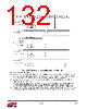
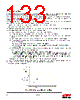
133 / 241 page  133 Rev 1.3 9.3.10. One-Pulse Mode One-pulse mode (OPM) is a special case of the previous modes. It allows the counter to be started in response to a stimulus and to generate a pulse with a programmable length after a programmable delay. Starting the counter can be controlled through the slave mode controller. Generating the waveform can be done in output compare mode or PWM mode. Select OPM by setting the TIM_OPM bit in the TIMx_CR1 register. This makes the counter stop automatically at the next UEV. A pulse can be correctly generated only if the compare value is different from the counter initial value. Before starting (when the timer is waiting for the trigger), the configuration must be: In up-counting: TIMx_CNT < TIMx_CCRy ? TIMx_ARR (in particular, 0 < TIMx_CCRy), In down-counting: TIMx_CNT > TIMx_CCRy. For example, to generate a positive pulse on OC1 with a length of tPULSE and after a delay of tDELAY as soon as a rising edge is detected on the TI2 input pin, using TI2FP2 as trigger 1: Map TI2FP2 on TI2: Write TIM_IC2S = 01 in the TIMx_CCMR1 register. TI2FP2 must detect a rising edge. Write TIM_CC2P = 0 in the TIMx_CCER register. Configure TI2FP2 as trigger for the slave mode controller (TRGI): Write TIM_TS = 110 in the TIMx_SMCR register. Use TI2FP2 to start the counter: Write TIM_SMS to 110 in the TIMx_SMCR register (trigger mode). The OPM waveform is defined: Write the compare registers, taking into account the clock frequency and the counter prescaler. The tDELAY is defined by the value written in the TIMx_CCR1 register. The tPULSE is defined by the difference between the auto-reload value and the compare value (TIMx_ARR - TIMx_CCR1). To build a waveform with a transition from 0 to 1 when a compare match occurs and a transition from 1 to 0 when the counter reaches the auto-reload value: Enable PWM mode 2: Write TIM_OC1M = 111 in the TIMx_CCMR1 register. Optionally, enable the buffer registers: Write TIM_OC1BE = 1 in the TIMx_CCMR1 register and TIM_ARBE in the TIMx_CR1 register. In this case, also write the compare value in the TIMx_CCR1 register, the auto-reload value in the TIMx_ARR register, generate an update by setting the TIM_UG bit, and wait for external trigger event on TI2. TIM_CC1P is written to 0 in this example. In the example, the TIM_DIR and TIM_CMS bits in the TIMx_CR1 register should be low. Since only one pulse is desired, software should set the TIM_OPM bit in the TIMx_CR1 register to stop the counter at the next UEV (when the counter rolls over from the auto-reload value back to 0). Figure 9.24 illustrates this example. Figure 9.24. Example of One Pulse Mode |
|
链接网址 |
| ALLDATASHEET是否为您带来帮助? [ DONATE ] |
关于 Alldatasheet | 广告服务 | 联系我们 | 隐私政策 | 数据表链接 | 链接交换 | 制造商名单 All Rights Reserved©Alldatasheet.com |
| Russian : Alldatasheetru.com | Korean : Alldatasheet.co.kr | Spanish : Alldatasheet.es | French : Alldatasheet.fr | Italian : Alldatasheetit.com Portuguese : Alldatasheetpt.com | Polish : Alldatasheet.pl | Vietnamese : Alldatasheet.vn Indian : Alldatasheet.in | Mexican : Alldatasheet.com.mx | British : Alldatasheet.co.uk | New Zealand : Alldatasheet.co.nz |
|
Family Site : ic2ic.com |
icmetro.com |
 Chinese ▼
 English
 Chinese
 German
 Japanese
 Russian
 Korean
 Spanish
 French
 Italian
 Portuguese
 Polish
 Vietnamese
 Indian
 Mexican
 British
 New Zealand