|
数据搜索系统,热门电子元器件搜索 |
|
|
数据搜索系统,热门电子元器件搜索 |
|
EM357-RTR 数据表(PDF) 154 Page - Silicon Laboratories |
|
|
|||||||||||||||||||||||||||||
EM357-RTR 数据表(HTML) 154 Page - Silicon Laboratories |
|
|
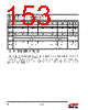
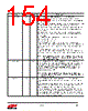
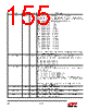
154 / 241 page  Rev 1.3 154 Bitname Bitfield Access Description TIM_OC2M [14:12] RW Output Compare 2 Mode. (Applies only if TIM_CC2S = 0.) Define the behavior of the output reference signal OC2REF from which OC2 derives. OC2REF is active high whereas OC2''s active level depends on the TIM_CC2P bit. 000: Frozen - The comparison between the output compare register TIMx- _CCR2 and the counter TIMx_CNT has no effect on the outputs. 001: Set OC2REF to active on match. The OC2REF signal is forced high when the counter TIMx_CNT matches the capture/compare register 2 (TIMx_CCR2) 010: Set OC2REF to inactive on match. OC2REF signal is forced low when the counter TIMx_CNT matches the capture/compare register 2 (TIMx_CCR2). 011: Toggle - OC2REF toggles when TIMx_CNT = TIMx_CCR2. 100: Force OC2REF inactive. 101: Force OC2REF active. 110: PWM mode 1 - In up-counting, OC2REF is active as long as TIMx_CNT < TIMx_CCR2, otherwise OC2REF is inactive. In down-count- ing, OC2REF is inactive if TIMx_CNT > TIMx_CCR2, otherwise OC2REF is active. 111: PWM mode 2 - In up-counting, OC2REF is inactive if TIMx_CNT < TIMx_CCR2, otherwise OC2REF is active. In down-count- ing, OC2REF is active if TIMx_CNT > TIMx_CCR2, otherwise it is inactive. Note: In PWM mode 1 or 2, the OC2REF level changes only when the result of the comparison changes or when the output compare mode switches from “frozen” mode to “PWM” mode. TIM_OC2BE [11] RW Output Compare 2 Buffer Enable. (Applies only if TIM_CC2S = 0.) 0: Buffer register for TIMx_CCR2 is disabled. TIMx_CCR2 can be written at anytime, the new value is used by the shadow register immediately. 1: Buffer register for TIMx_CCR2 is enabled. Read/write operations access the buffer register. TIMx_CCR2 buffer value is loaded in the shadow register at each UEV. Note: The PWM mode can be used without enabling the buffer register only in one pulse mode (TIM_OPM bit set in the TIMx_CR2 register), otherwise the behavior is undefined. TIM_OC2FE [10] RW Output Compare 2 Fast Enable. (Applies only if TIM_CC2S = 0.) This bit speeds the effect of an event on the trigger in input on the OC2 output. 0: OC2 behaves normally depending on the counter and TIM_CCR2 val- ues even when the trigger is ON. The minimum delay to activate OC2 when an edge occurs on the trigger input is 5 clock cycles. 1: An active edge on the trigger input acts like a compare match on the OC2 output. OC2 is set to the compare level independently from the result of the comparison. Delay to sample the trigger input and to activate OC2 output is reduced to 3 clock cycles. TIM_OC2FE acts only if the channel is configured in PWM 1 or PWM 2 mode. |
|
链接网址 |
| ALLDATASHEET是否为您带来帮助? [ DONATE ] |
关于 Alldatasheet | 广告服务 | 联系我们 | 隐私政策 | 数据表链接 | 链接交换 | 制造商名单 All Rights Reserved©Alldatasheet.com |
| Russian : Alldatasheetru.com | Korean : Alldatasheet.co.kr | Spanish : Alldatasheet.es | French : Alldatasheet.fr | Italian : Alldatasheetit.com Portuguese : Alldatasheetpt.com | Polish : Alldatasheet.pl | Vietnamese : Alldatasheet.vn Indian : Alldatasheet.in | Mexican : Alldatasheet.com.mx | British : Alldatasheet.co.uk | New Zealand : Alldatasheet.co.nz |
|
Family Site : ic2ic.com |
icmetro.com |
 Chinese ▼
 English
 Chinese
 German
 Japanese
 Russian
 Korean
 Spanish
 French
 Italian
 Portuguese
 Polish
 Vietnamese
 Indian
 Mexican
 British
 New Zealand