|
数据搜索系统,热门电子元器件搜索 |
|
|
数据搜索系统,热门电子元器件搜索 |
|
EM357-RTR 数据表(PDF) 173 Page - Silicon Laboratories |
|
|
|||||||||||||||||||||||||||||
EM357-RTR 数据表(HTML) 173 Page - Silicon Laboratories |
|
|
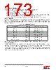
173 / 241 page  173 Rev 1.3 10.1. Setup and Configuration To use the ADC follow this procedure, described in more detail in the next sections: Configure any GPIO pins to be used by the ADC in analog mode. Configure the voltage reference (internal or external). Set the offset and gain values. If using DMA, reset the ADC DMA, define the DMA buffer, and start the DMA in the proper transfer mode. If interrupts will be used, configure the top-level and second-level ADC interrupt bits. Write the ADC configuration register to define the inputs, sample time, and start the conversions. 10.1.1. GPIO Usage A GPIO pin used by the ADC as an input or voltage reference must be configured in analog mode by writing 0 to its 4-bit field in the proper GPIO_PxCFGH/L register. Note that a GPIO pin in analog mode cannot be used for any digital functions, and GPIO_PxIN always reads it as 1. Only certain pins can be configured in analog mode. These are listed in Table 10.1. See "7. GPIO (General Purpose Input/Output)" on page 50 for more information about how to configure GPIO. 10.1.2. Voltage Reference The ADC voltage reference (VREF), may be internally generated or externally sourced from PB0. If internally generated, it may optionally be output on PB0. To output the internal VREF on PB0, the ADC must be enabled (ADC_ENABLE bit set in the ADC_CFG register) and PB0 must be configured in analog mode. To use an external reference, the Ember software must be called after reset and after waking from deep sleep. PB0 must also be configured in analog mode using GPIO_PBCFGH[3:0]. See the Ember software documentation for more information on using an external reference. Table 10.1. ADC GPIO Pin Usage Analog Signal GPIO Configuration control ADC0 input PB5 GPIO_PBCFGH[7:4] ADC1 input PB6 GPIO_PBCFGH[11:8] ADC2 input PB7 GPIO_PBCFGH[15:12] ADC3 input PC1 GPIO_PCCFGL[7:4] ADC4 input PA4 GPIO_PACFGH[3:0] ADC5 input PA5 GPIO_PACFGH[7:4] VREF input or output PB0 GPIO_PBCFGL[3:0] |
|
链接网址 |
| ALLDATASHEET是否为您带来帮助? [ DONATE ] |
关于 Alldatasheet | 广告服务 | 联系我们 | 隐私政策 | 数据表链接 | 链接交换 | 制造商名单 All Rights Reserved©Alldatasheet.com |
| Russian : Alldatasheetru.com | Korean : Alldatasheet.co.kr | Spanish : Alldatasheet.es | French : Alldatasheet.fr | Italian : Alldatasheetit.com Portuguese : Alldatasheetpt.com | Polish : Alldatasheet.pl | Vietnamese : Alldatasheet.vn Indian : Alldatasheet.in | Mexican : Alldatasheet.com.mx | British : Alldatasheet.co.uk | New Zealand : Alldatasheet.co.nz |
|
Family Site : ic2ic.com |
icmetro.com |
 Chinese ▼
 English
 Chinese
 German
 Japanese
 Russian
 Korean
 Spanish
 French
 Italian
 Portuguese
 Polish
 Vietnamese
 Indian
 Mexican
 British
 New Zealand