|
数据搜索系统,热门电子元器件搜索 |
|
|
数据搜索系统,热门电子元器件搜索 |
|
EM357-RTR 数据表(PDF) 174 Page - Silicon Laboratories |
|
|
|||||||||||||||||||||||||||||
EM357-RTR 数据表(HTML) 174 Page - Silicon Laboratories |
|
|
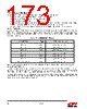
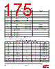
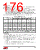
174 / 241 page  Rev 1.3 174 10.1.3. Offset/Gain Correction When a conversion is complete, the 16-bit converted data is processed in several steps by offset/gain correction hardware: 1. The initial signed ADC conversion result is added to the 16-bit signed (two's complement) value of the ADC offset register (ADC_OFFSET). 2. The offset-corrected data is multiplied by the 16-bit ADC gain register, ADC_GAIN, to produce a 16-bit signed result. If the product is greater than 0x7FFF (32767), or less than 0x8000 (–32768), it is limited to that value and the INT_ADCSAT bit is set in the INT_ADCFLAG register. 3. The offset/gain corrected value is divided by two to produce the final result. ADC_GAIN is an unsigned scaled 16-bit value: ADC_GAIN[15] is the integer part of the gain factor and ADC_GAIN[14:0] is the fractional part. As a result, ADC_GAIN values can represent gain factors from 0 through (2 - 2-15). Although ADC_GAIN can represent a much greater range, its purpose is to correct small gain error, and in practice is loaded with values within a range of about 0.95 to 1.05. Reset initializes the offset to zero (ADC_OFFSET = 0) and gain factor to one (ADC_GAIN = 0x8000). 10.1.4. DMA The ADC DMA channel writes converted data, which incorporates the offset/gain correction, into a DMA buffer in RAM. The ADC DMA buffer is defined by two registers: ADC_DMABEG is the start address of the buffer and must be even. ADC_DMASIZE specifies the size of the buffer in 16-bit samples, or half its length in bytes. To prepare the DMA channel for operation, reset it by writing the ADC_DMARST bit in the ADC_DMACFG register, then start the DMA in either linear or auto wrap mode by setting the ADC_DMALOAD bit in the ADC_DMACFG register. The ADC_DMAAUTOWRAP bit in the ADC_DMACFG register selects the DMA mode: 0 for linear mode, 1 for auto wrap mode. In linear mode the DMA writes to the buffer until the number of samples given by ADC_DMASIZE has been output. The DMA then stops and sets the INT_ADCULDFULL bit in the INT_ADCFLAG register. If another ADC conversion completes before the DMA is reset or the ADC is disabled, the INT_ADCOVF bit in the INT_ADCFLAG register is set. In auto wrap mode the DMA writes to the buffer until it reaches the end, then resets its pointer to the start of the buffer and continues writing samples. The DMA transfers continue until the ADC is disabled or the DMA is reset. When the DMA fills the lower and upper halves of the buffer, it sets the INT_ADCULDHALF and INT_ADCULDFULL bits, respectively, in the INT_ADCFLAG register. The current location to which the DMA is writing can also be determined by reading the ADC_DMACUR register. 10.1.5. ADC Configuration Register The ADC configuration register (ADC_CFG) sets up most of the ADC operating parameters. 10.1.5.1. Input The analog input of the ADC can be chosen from various sources. The analog input is configured with the ADC_MUXP and ADC_MUXN bits within the ADC_CFG register. Table 10.2 shows the possible input selections. |
|
链接网址 |
| ALLDATASHEET是否为您带来帮助? [ DONATE ] |
关于 Alldatasheet | 广告服务 | 联系我们 | 隐私政策 | 数据表链接 | 链接交换 | 制造商名单 All Rights Reserved©Alldatasheet.com |
| Russian : Alldatasheetru.com | Korean : Alldatasheet.co.kr | Spanish : Alldatasheet.es | French : Alldatasheet.fr | Italian : Alldatasheetit.com Portuguese : Alldatasheetpt.com | Polish : Alldatasheet.pl | Vietnamese : Alldatasheet.vn Indian : Alldatasheet.in | Mexican : Alldatasheet.com.mx | British : Alldatasheet.co.uk | New Zealand : Alldatasheet.co.nz |
|
Family Site : ic2ic.com |
icmetro.com |
 Chinese ▼
 English
 Chinese
 German
 Japanese
 Russian
 Korean
 Spanish
 French
 Italian
 Portuguese
 Polish
 Vietnamese
 Indian
 Mexican
 British
 New Zealand