|
数据搜索系统,热门电子元器件搜索 |
|
|
数据搜索系统,热门电子元器件搜索 |
|
EM357-RTR 数据表(PDF) 178 Page - Silicon Laboratories |
|
|
|||||||||||||||||||||||||||||
EM357-RTR 数据表(HTML) 178 Page - Silicon Laboratories |
|
|
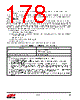
178 / 241 page  Rev 1.3 178 6. Wait until the INT_ADCULDFULL bit is set in the INT_ADCFLAG register, then read the result from analogData. To convert multiple inputs using this approach, repeat steps 4 through 6, loading the desired input configurations to the ADC_CFG register in Step 5. If the inputs can use the same offset/gain correction, just repeat steps 5 and 6. 10.4. Calibration Sampling of internal connections GND, VREF/2, and VREF allow for offset and gain calibration of the ADC in applications where absolute accuracy is important. Offset error is calculated from the minimum input, and gain error is calculated from the full-scale input range. Correction using VREF is recommended because VREF is calibrated by the Ember software against VDD_PADSA. The VDD_PADSA regulator is factory-trimmed to 1.80 V ±20 mV. If better absolute accuracy is required, the ADC can be configured to use an external reference. The ADC calibrates as a single-ended measurement. Differential signals require correction of both their inputs. The following steps outline the calibration procedure: 1. Calibrate VREF against VDD_PADSA. 2. Determine the ADC gain by sampling independently VREF and GND. Gain is calculated from the slope of these two measurements. 3. Apply gain correction. 4. Determine the ADC offset by sampling GND. 5. Apply offset correction. Table 10.5 shows the equations used to calculate the gain and offset correction values. Table 10.5. ADC Gain and Offset Correction Equations Calibration Correction Value Gain Offset (after applying gain correction) Notes: 1. The ADC output is 2s complement. All N are therefore 16-bit 2s complement numbers. 2. Offset is a 16-bit 2s complement number. 3. Gain is a 16-bit number representing a gain of 0 to 65535/32768 in 1/32768 steps. The default value is 32768, corresponding to a gain of 1. 4. NGND is a sampling of ground. Due to the ADC's internal design, VGND does not yield the minimum 16 bit 2s complement value 32768 as the conversion result. Instead, VGND yields a value close to 57344 when the input buffer is not selected. VGND cannot be measured when the input buffer is enabled because it is outside the buffer's input range. 5. NVREF is a sampling of VREF. Due to the ADC's internal design, VREF does not yield the maximum positive 16-bit 2s complement 32767 as the conversion result. Instead, VREF yields a value close to 8192. 6. NVREF/2 is a sampling of VREF/2. VREF/2 yields a value close to 0. 7. Offset correction is affected by the gain correction value. Offset correction is calculated after gain correction has been applied. 32768 16384 NVREF NGND – -------------------------------------------- 2 57344 NGND – |
|
链接网址 |
| ALLDATASHEET是否为您带来帮助? [ DONATE ] |
关于 Alldatasheet | 广告服务 | 联系我们 | 隐私政策 | 数据表链接 | 链接交换 | 制造商名单 All Rights Reserved©Alldatasheet.com |
| Russian : Alldatasheetru.com | Korean : Alldatasheet.co.kr | Spanish : Alldatasheet.es | French : Alldatasheet.fr | Italian : Alldatasheetit.com Portuguese : Alldatasheetpt.com | Polish : Alldatasheet.pl | Vietnamese : Alldatasheet.vn Indian : Alldatasheet.in | Mexican : Alldatasheet.com.mx | British : Alldatasheet.co.uk | New Zealand : Alldatasheet.co.nz |
|
Family Site : ic2ic.com |
icmetro.com |
 Chinese ▼
 English
 Chinese
 German
 Japanese
 Russian
 Korean
 Spanish
 French
 Italian
 Portuguese
 Polish
 Vietnamese
 Indian
 Mexican
 British
 New Zealand