|
数据搜索系统,热门电子元器件搜索 |
|
|
数据搜索系统,热门电子元器件搜索 |
|
ADP1050ACPZ-R7 数据表(PDF) 87 Page - Analog Devices |
|
|
|||||||||||||||||||||||||||||
ADP1050ACPZ-R7 数据表(HTML) 87 Page - Analog Devices |
|
|
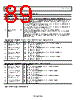
87 / 93 page  ADP1050 Data Sheet DUTY CYCLE READING SETTING REGISTERS Table 148. Register 0xFE58—Duty Cycle Reading Settings Bits Bit Name/Function R/W Description [7:4] Reserved R/W Reserved. 3 OUTB duty cycle reporting R/W 1 = READ_DUTY_CYCLE reports OUTB duty cycle value. 2 OUTA duty cycle reporting R/W 1 = READ_DUTY_CYCLE reports OUTA duty cycle value. 1 Reserved R/W Reserved. 0 Polarity setting for input voltage compensation R/W Setting this bit applies an offset on the input voltage reading, READ_VIN, based on the reading of the input current, READ_IIN. The compensation multipler is set in Register 0xFE59. It is used to compensate the voltage drop caused by the current conduction. 0 = positive polarity compensation. 1 = negative polarity compensation. Table 149. Register 0xFE59—Input Voltage Compensation Multiplier Bits Bit Name/Function R/W Description [7:0] Input voltage compensation multiplier R/W These bits specify the multiplier, N, for the input voltage compensation coefficient. The compensation equation is N × (Register 0xFEA7[15:4] value) ÷ 211, and the result is added to Register 0xFEAC[15:5]. The compensation polarity is set by Register 0xFE58[0]. OTHER REGISTER SETTINGS Table 150. Register 0xFE61—Go Commands Bits Bit Name/Function R/W Description [7:3] Reserved R/W Reserved. 2 Frequency go R/W This bit synchronously latches the contents of Register 0x33 into the shadow registers used to calculate the switching frequency. Reading of this bit always returns 1. 1 PWM setting go R/W This bit synchronously latches the contents of Registers 0xFE3E to Register 0xFE53 into the shadow registers used to calculate the PWM edge timing. Reading this bit always returns 1. 0 Reserved R/W Reserved. Table 151. Register 0xFE62—Customized Register Bits Bit Name/Function R/W Description [7:0] Customized register R/W These bits are available to the user to store customized information. Table 152. Register 0xFE63—Modulation Reference MSBs Setting for Open-Loop Input Voltage Feedforward Operation Bits Bit Name/Function R/W Description [7:0] Modulation reference setting MSBs R/W This register sets the eight MSBs of the modulation reference in open-loop feedforward operation mode. The step size of an LSB depends on the switching frequency. Switching Frequency Range (kHz) LSB Step Size (ns) 49 to 87 80 97.5 to 184 40 195.5 to 379 20 390.5 to 625 10 Table 153. Register 0xFE64—Modulation Reference LSBs Setting for Open-Loop Input Voltage Feedforward Operation Bits Bit Name/Function R/W Description [7:0] Modulation reference setting LSBs R/W This register sets the eight LSBs of the modulation reference in open-loop feedforward operation mode. The step size of an LSB depends on the switching frequency. Switching Frequency Range (kHz) LSB Step Size (ps) 49 to 87 312.5 97.5 to 184 156.25 195.5 to 379 78.125 390.5 to 625 39.0625 Rev. A | Page 86 of 92 |
|
链接网址 |
| ALLDATASHEET是否为您带来帮助? [ DONATE ] |
关于 Alldatasheet | 广告服务 | 联系我们 | 隐私政策 | 数据表链接 | 链接交换 | 制造商名单 All Rights Reserved©Alldatasheet.com |
| Russian : Alldatasheetru.com | Korean : Alldatasheet.co.kr | Spanish : Alldatasheet.es | French : Alldatasheet.fr | Italian : Alldatasheetit.com Portuguese : Alldatasheetpt.com | Polish : Alldatasheet.pl | Vietnamese : Alldatasheet.vn Indian : Alldatasheet.in | Mexican : Alldatasheet.com.mx | British : Alldatasheet.co.uk | New Zealand : Alldatasheet.co.nz |
|
Family Site : ic2ic.com |
icmetro.com |
 Chinese ▼
 English
 Chinese
 German
 Japanese
 Russian
 Korean
 Spanish
 French
 Italian
 Portuguese
 Polish
 Vietnamese
 Indian
 Mexican
 British
 New Zealand