|
数据搜索系统,热门电子元器件搜索 |
|
|
数据搜索系统,热门电子元器件搜索 |
|
ADP1050ACPZ-R7 数据表(PDF) 23 Page - Analog Devices |
|
|
|||||||||||||||||||||||||||||
ADP1050ACPZ-R7 数据表(HTML) 23 Page - Analog Devices |
|
|
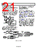
23 / 93 page  ADP1050 Data Sheet Rev. A | Page 22 of 92 Power-Good Signals The ADP1050 has an open-drain, power-good pin, PG (PG/ALT, Pin 14). When the pin is logic high, the power is good. The ADP1050 also has a power-good flag, PGOOD, which is a negation of power good. When this flag is set, it indicates that the power is not good. The PG/ALT pin and the PGOOD flag can be programmed to respond to the flags from the following list: VIN_UV_FAULT IIN_OC_FAST_FAULT VOUT_OV_FAULT VOUT_UV_FAULT OT_FAULT OT_WARNING Register 0xFE0D is used to program the masking of these flags, which prevents them from setting the PGOOD flag and driving the PG/ALT pin low. Register 0xFE0E[1:0] is used to set the debounce time to drive the PG/ALT pin low and set the PGOOD flag (see Figure 26). The POWER_GOOD_ON command (Register 0x5E) sets the voltage limit that the output voltage must exceed before the POWER_GOOD flag (Register 0x79[11]) can be cleared. Simi- larly, the output voltage must fall below the POWER_GOOD_ OFF limit (Register 0x5F) for the POWER_GOOD flag to be set. The PG/ALT pin is always driven low and the PGOOD flag is always set when one of the POWER_OFF, SOFT_START_FILTER, CRC_FAULT, or POWER_GOOD flags is set. The debounce timings for setting and clearing the PGOOD flag can be programmed to 0 ms, 200 ms, 320 ms, or 600 ms in Register 0xFE0E[3:0]. VOLT-SECOND BALANCE CONTROL The ADP1050 has a dedicated circuit to maintain volt-second balance in the main transformer when operating in full bridge topology. This circuit eliminates the need for a dc blocking capacitor. In interleaved topologies, volt-second balance can also be used for current balancing to ensure that each interleaved phase contributes equal power. The circuit monitors the current flowing in both legs of the full bridge topology and stores this information. It compensates the selected PWM signals to ensure equal current flow in the two legs of the full bridge topology. The CS1 pin is used as the input for this function. Several switching cycles are required for the circuit to operate effectively. The maximum amount of modulation applied to each edge of the selected PWM outputs is programmable to ±80 ns or ±160 ns, using Register 0xFE54[2]. The balance control gains are programmable via Register 0xFE54[1:0]. The compensation of the PWM drive signals is performed on the edges of two selected outputs, using Register 0xFE55 and Register 0xFE57. The direction of the modulation is also programmable in these registers. The volt-second balance control can be disabled during soft start using Register 0xFE0C[1]. There are also leading edge blanking functions at the sensed CS1 signal for more accurate control results. The blanking time follows the CS1 cycle-by-cycle current-limit blanking time (see the CS1 Current Sense section). To avoid the wrong compensation in light load condition, there is a CS1 threshold in Register 0xFE38 to enable volt-second balance. Below this threshold, volt-second balance is not enabled. DEBOUNCE DEBOUNCE DEBOUNCE DEBOUNCE DEBOUNCE VIN_UV_FAULT IIN_OC_FAST_FAULT DEBOUNCE REG 0xFE0D REG 0xFE0F REG 0xFE0E[3:0] DEBOUNCE PGOOD FLAG REG 0xFEA0[6] PG/ALT PIN VOUT_OV_FAULT VOUT_UV_FAULT OT_FAULT OT_WARNING POWER_OFF SOFT_START_FILTER CRC_FAULT POWER_GOOD Figure 26. PGOOD Programming |
|
链接网址 |
| ALLDATASHEET是否为您带来帮助? [ DONATE ] |
关于 Alldatasheet | 广告服务 | 联系我们 | 隐私政策 | 数据表链接 | 链接交换 | 制造商名单 All Rights Reserved©Alldatasheet.com |
| Russian : Alldatasheetru.com | Korean : Alldatasheet.co.kr | Spanish : Alldatasheet.es | French : Alldatasheet.fr | Italian : Alldatasheetit.com Portuguese : Alldatasheetpt.com | Polish : Alldatasheet.pl | Vietnamese : Alldatasheet.vn Indian : Alldatasheet.in | Mexican : Alldatasheet.com.mx | British : Alldatasheet.co.uk | New Zealand : Alldatasheet.co.nz |
|
Family Site : ic2ic.com |
icmetro.com |
 Chinese ▼
 English
 Chinese
 German
 Japanese
 Russian
 Korean
 Spanish
 French
 Italian
 Portuguese
 Polish
 Vietnamese
 Indian
 Mexican
 British
 New Zealand