|
数据搜索系统,热门电子元器件搜索 |
|
|
数据搜索系统,热门电子元器件搜索 |
|
ADP1050ACPZ-R7 数据表(PDF) 20 Page - Analog Devices |
|
|
|||||||||||||||||||||||||||||
ADP1050ACPZ-R7 数据表(HTML) 20 Page - Analog Devices |
|
|
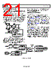
20 / 93 page  Data Sheet ADP1050 OPEN-LOOP INPUT VOLTAGE FEEDFORWARD OPERATION The ADP1050 can run in open-loop input voltage feedforward operation mode. In this mode, the input voltage is sensed as the feedforward signal for the generation of the PWM outputs. As shown in Figure 22, the digital compensator output is modified by a programmable modulation reference. The VF value, which represents the input voltage, is fed into the feedforward ADC to divide the modulation reference. The result of this division is then fed into the PWM engine. The duty cycle value is in inverse proportion to the input voltage. DPWM ENGINE VF 1/x Σ-Δ ADC READ_VIN REG 0x88 REG 0x35, REG 0x36 FEED- FORWARD ADC 0.5V TO 1.6V 0V TO 1.6V VIN_LOW FLAG REG 0x7C[3] REG 0xFE29[5] VIN_UV_FAULT FLAG REG 0x7C[4] FROM THE VIN SENSE CIRCUIT MODULATION REFERENCE REG 0xFE63 AND REG 0xFE64 Figure 22. Open-Loop Feedforward Operation Use the following equations to derive the output voltage equation: D = IN NOM IN V V _ × (tREF × fSW) and VOUT = n D V IN × The output voltage can then be derived by VOUT = ( ) n f t V SW REF NOM IN × × _ where: D is the duty cycle value. VIN_NOM is the nominal input voltage. VIN is the input voltage. VOUT is the output voltage. n is the turns ratio of the main transformer. tREF is the modulation reference, which is set by Register 0xFE63 and Register 0xFE64. fSW is the switching frequency. In the equation to derive VOUT, the input voltage, VIN, is cancelled out. Therefore, the output voltage does not change when the input voltage changes. Register 0xFE63 and Register 0xFE64 set the modulation reference, based on the target output voltage and the nominal input voltage at which the VF pin voltage is 1 V (see Figure 22). The PWM settings for open-loop input voltage feedforward operation are similar to those of general closed-loop operation. The falling edge timings, rising edge timings, and modulation are set in the same manner as for closed-loop operation, by using Register 0xFE3E to Register 0xFE52. Register 0xFE09[4:3] sets the soft start speed of the modulation edges. Register 0xFE3D[6] enables open-loop feed- forward operation. Register 0xFE3D[7] is used to enable the soft start procedure for open-loop feedforward operation. The flag settings for open-loop feedforward operation are also similar to those of general closed-loop operation. Because the output voltage is not regulated in the same manner as in closed-loop operation, some settings, such as the VOUT setting, the digital compensator settings, and the constant current mode setting, are not functional. Other settings can be programmed in a manner that is similar to general closed-loop operation. OPEN-LOOP OPERATION The ADP1050 can also run in open-loop operation mode. In this mode, the rising edges and falling edges of the PWM outputs are fixed during normal operation. Therefore, the output voltage varies with the input voltage. The topologies include full bridge, half bridge, and push pull converters. The PWM settings for open-loop operation are different from those of general closed-loop operation. 1. Set the rising edge timings and falling edge timings using Register 0xFE3E to Register 0xFE4F. Typically, a duty cycle setting of ~50% is recommended for ease of zero voltage switching operation. A phase shift function of 180° is recommended to guarantee balanced PWM outputs. 2. Program Register 0xFE3C to a value of 0x00, which sets the modulation limit to 0 µs. 3. For soft start, apply negative modulation to the falling edges of the OUTA and OUTB outputs. The soft start of SR1 and SR2 is not recommended. 4. Write 111111 to Register 0xFE67[5:4] and Register 0xFE67[1:0] to set all PWM channels to follow open-loop operation. Set Register 0xFE09[7] to enable the soft start procedure. The soft start speed is specified by Register 0xFE09[4:3]. 5. Always set Register 0xFE09[2] = 1. The soft start ramp time is determined by tF2 − tR2. Because the output voltage is not regulated, some of the settings, such as the VOUT setting, digital compensator settings, and constant current control, are not functional. Other settings can be pro- grammed to be similar to those of general closed-loop operation. Rev. A | Page 19 of 92 |
|
链接网址 |
| ALLDATASHEET是否为您带来帮助? [ DONATE ] |
关于 Alldatasheet | 广告服务 | 联系我们 | 隐私政策 | 数据表链接 | 链接交换 | 制造商名单 All Rights Reserved©Alldatasheet.com |
| Russian : Alldatasheetru.com | Korean : Alldatasheet.co.kr | Spanish : Alldatasheet.es | French : Alldatasheet.fr | Italian : Alldatasheetit.com Portuguese : Alldatasheetpt.com | Polish : Alldatasheet.pl | Vietnamese : Alldatasheet.vn Indian : Alldatasheet.in | Mexican : Alldatasheet.com.mx | British : Alldatasheet.co.uk | New Zealand : Alldatasheet.co.nz |
|
Family Site : ic2ic.com |
icmetro.com |
 Chinese ▼
 English
 Chinese
 German
 Japanese
 Russian
 Korean
 Spanish
 French
 Italian
 Portuguese
 Polish
 Vietnamese
 Indian
 Mexican
 British
 New Zealand