|
数据搜索系统,热门电子元器件搜索 |
|
|
数据搜索系统,热门电子元器件搜索 |
|
H8SX1663 数据表(PDF) 350 Page - Renesas Technology Corp |
|
|
|||||||||||||||||||||||||||||
H8SX1663 数据表(HTML) 350 Page - Renesas Technology Corp |
|
|
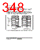
350 / 1158 page  Section 6 Bus Controller (BSC) Rev.1.00 Jun. 07, 2006 Page 298 of 1102 REJ09B0294-0100 (6) Relationship between Chip Select ( CS) Signal and Read (RD) Signal Depending on the system's load conditions, the RD signal may lag behind the CS signal. An example is shown in figure 6.95. In this case, with the setting for no idle cycle insertion (a), there may be a period of overlap between the RD signal in bus cycle A and the CS signal in bus cycle B. Setting idle cycle insertion, as in (b), however, will prevent any overlap between the RD and CS signals. In the initial state after reset release, idle cycle indicated in (b) is set. Bus cycle A Bus cycle B B φ Address bus CS (area A) CS (area B) RD T 1 T 2 T 3 T 1 T 2 Bus cycle A Bus cycle B T 1 T 2 T 3 T 1 T i T 2 Overlap time may occur between the CS (area B) and RD (a) No idle cycle inserted (IDLS1 = 0) (b) Idle cycle inserted (IDLS1 = 1, IDLSELn = 0, IDLCA1 = 0, IDLCA0 = 0) Figure 6.95 Relationship between Chip Select ( CS) and Read (RD) |
|
链接网址 |
| ALLDATASHEET是否为您带来帮助? [ DONATE ] |
关于 Alldatasheet | 广告服务 | 联系我们 | 隐私政策 | 数据表链接 | 链接交换 | 制造商名单 All Rights Reserved©Alldatasheet.com |
| Russian : Alldatasheetru.com | Korean : Alldatasheet.co.kr | Spanish : Alldatasheet.es | French : Alldatasheet.fr | Italian : Alldatasheetit.com Portuguese : Alldatasheetpt.com | Polish : Alldatasheet.pl | Vietnamese : Alldatasheet.vn Indian : Alldatasheet.in | Mexican : Alldatasheet.com.mx | British : Alldatasheet.co.uk | New Zealand : Alldatasheet.co.nz |
|
Family Site : ic2ic.com |
icmetro.com |
 Chinese ▼
 English
 Chinese
 German
 Japanese
 Russian
 Korean
 Spanish
 French
 Italian
 Portuguese
 Polish
 Vietnamese
 Indian
 Mexican
 British
 New Zealand