|
数据搜索系统,热门电子元器件搜索 |
|
|
数据搜索系统,热门电子元器件搜索 |
|
PC87373 数据表(PDF) 73 Page - National Semiconductor (TI) |
|
|
|
|||||||||||||||||||||||||||||
PC87373 数据表(HTML) 73 Page - National Semiconductor (TI) |
|
|
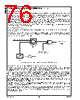
73 / 174 page  73 www.national.com Revision 1.1 5.0 General-Purpose Input/Output (GPIO) Ports This chapter describes one 8-bit port. A device may include a combination of several ports with different implementations. For device specific implementation, see Section 3.14 on page 62. 5.1 OVERVIEW The GPIO port is an 8-bit port, connected to eight pins. It features: • Software capability to control and read pin levels. • Flexible system notification by several means, based on the pin level or level transition. • Ability to capture and route events and their associated status. • Back-drive protected pins. GPIO port operation is associated with two sets of registers: • Pin Configuration registers mapped in the Device Configuration space. These registers are used to configure the logical behavior of each pin. There are three registers for each GPIO pin: GPIO Pin Configuration registers 1 and 2 (GPCFG1, GPCFG2) and the GPIO Pin Event Routing register (GPEVR). • Four 8-bit runtime registers: GPIO Data Out (GPDO), GPIO Data In (GPDI), GPIO Event Enable (GPEVEN) and GPIO Event Status (GPEVST). These registers are mapped in the GPIO device I/O space (which is determined by the base address registers in the GPIO Device Configuration). They are used to control and/or read the pin values and to handle system notification. Each runtime register corresponds to the 8-pin port, such that bit ‘n’ in each one of the four registers is associated with GPIOXn pin, where ‘X’ is the port number. • An additional optional runtime register: GPIO Data In/Out (GPDIO). This register is also mapped in the GPIO device I/O space, but at a separate location from the above group of four runtime registers. It contains the same data-out value as the GPDO register and the same data-in value as the GPDI register. Each GPIO pin is associated with configuration bits and the corresponding bit slice of the four runtime registers, as shown in Figure 9. Figure 9. GPIO Port Architecture GPIO Pin GPIO Pin Select (GPSEL) Configuration 1 and 2 GPDOX GPDIX GPEVENX GPEVSTX Runtime Registers GPIOX Base Address Event Bit n Port and Pin 8 GPCFG Registers x8 GPIOXn Pin x8 GPIOXn CNFG Interrupt Request x8 GPIOXn Port Logic X = port number n = pin number (0 to 7) Pending Indication GPIO Pin Event Routing (GPEVR) 8 GPEVR Registers GPIOXn ROUTE Select Event Routing Control Registers Register Register (GPCFG1 and GPCFG2) SWC SIOPME GPIO GPDIOX |
|
链接网址 |
| ALLDATASHEET是否为您带来帮助? [ DONATE ] |
关于 Alldatasheet | 广告服务 | 联系我们 | 隐私政策 | 数据表链接 | 链接交换 | 制造商名单 All Rights Reserved©Alldatasheet.com |
| Russian : Alldatasheetru.com | Korean : Alldatasheet.co.kr | Spanish : Alldatasheet.es | French : Alldatasheet.fr | Italian : Alldatasheetit.com Portuguese : Alldatasheetpt.com | Polish : Alldatasheet.pl | Vietnamese : Alldatasheet.vn Indian : Alldatasheet.in | Mexican : Alldatasheet.com.mx | British : Alldatasheet.co.uk | New Zealand : Alldatasheet.co.nz |
|
Family Site : ic2ic.com |
icmetro.com |
 Chinese ▼
 English
 Chinese
 German
 Japanese
 Russian
 Korean
 Spanish
 French
 Italian
 Portuguese
 Polish
 Vietnamese
 Indian
 Mexican
 British
 New Zealand