|
数据搜索系统,热门电子元器件搜索 |
|
|
数据搜索系统,热门电子元器件搜索 |
|
PC87373 数据表(PDF) 75 Page - National Semiconductor (TI) |
|
|
|
|||||||||||||||||||||||||||||
PC87373 数据表(HTML) 75 Page - National Semiconductor (TI) |
|
|
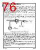
75 / 174 page  5.0 General-Purpose Input/Output (GPIO) Ports (Continued) 75 www.national.com Revision 1.1 The GPCFG2 register controls the Load Protection configuration option: • V DD-Powered Load: Disables the Output Buffer (if enabled), the Static Pull-Up (if enabled) and the Input Buffer if the specific GPIO pin is connected to a VDD-powered device and VDD3 power to the PC87373 is not present (No_Vdd). This function is controlled by the VDD-powered Load bit (bit 4). 5.2.2 Operation If the output is enabled, the value that is written to the GPDO or GPDIO registers is driven to the pin. Reading from the GPDO register returns its contents regardless of the actual pin value or the port configuration. The GPDI register is a read-only register. Reading from the GPDI register returns the actual pin value regardless of its source (the port itself or an external device). Writing to this register is ignored. Reading from the GPDIO register returns the actual pin value regardless of its source. Activation of the GPIO module is controlled by device-specific configuration bits. When this module is inactive, access through the LPC bus to the runtime registers (GPDI, GPDO and GPDIO) is disabled; however, there is no change in the GPDO and GPDIO values and therefore there is no effect on the outputs of the pins. The configuration and data registers of each GPIO pin are reset according to the setting of VDDLOAD bit in GPCFG2 reg- ister (see Section 3.14.6 on page 66). 5.3 EVENT HANDLING AND SYSTEM NOTIFICATION The enhanced GPIO port (GPIOE) supports system notification based on event detection. This functionality is based on configuration bits and a bit slice of runtime registers GPEVEN and GPEVST. The configuration and operation of the event detection capability is shown in Figure 11. System notification is described in Section 5.3.2. Figure 11. Event Detection 5.3.1 Event Configuration Each pin in the GPIO port is a potential input event source. The event detection can trigger a system notification upon prede- termined behavior of the source pin. The GPCFG1 register determines the event detection trigger type for system notification. Event Debounce Enable The input signal can be debounced for at least 16 ms, before entering the detector. To ensure that the signal is stable, the signal state is transferred to the event detector only after a debouncing period during which the signal has no transitions. The debouncer adds a delay equal to the debouncing period to both assertion and de-assertion of the event pending indi- cator (IRQ, SCI). The debounce is controlled by Event Debounce Enable (bit 6 of GPCFG1 register). Event Enable Event Polarity Input Debouncer 1 0 Event Internal Bus 0 1 Pin Level =1 Write 1 to Clear Status Rising Edge or Rising Edge Detector High Level =1 GPIO Pin Configuration Register 1 Event Type Event Debounce Enable R/W Bit 6 Bit 5 Bit 4 Indication Pending (GPCFG1) Reset Set GPIO Event Indication to SWC Read GPIO GPIO |
|
链接网址 |
| ALLDATASHEET是否为您带来帮助? [ DONATE ] |
关于 Alldatasheet | 广告服务 | 联系我们 | 隐私政策 | 数据表链接 | 链接交换 | 制造商名单 All Rights Reserved©Alldatasheet.com |
| Russian : Alldatasheetru.com | Korean : Alldatasheet.co.kr | Spanish : Alldatasheet.es | French : Alldatasheet.fr | Italian : Alldatasheetit.com Portuguese : Alldatasheetpt.com | Polish : Alldatasheet.pl | Vietnamese : Alldatasheet.vn Indian : Alldatasheet.in | Mexican : Alldatasheet.com.mx | British : Alldatasheet.co.uk | New Zealand : Alldatasheet.co.nz |
|
Family Site : ic2ic.com |
icmetro.com |
 Chinese ▼
 English
 Chinese
 German
 Japanese
 Russian
 Korean
 Spanish
 French
 Italian
 Portuguese
 Polish
 Vietnamese
 Indian
 Mexican
 British
 New Zealand