|
数据搜索系统,热门电子元器件搜索 |
|
|
数据搜索系统,热门电子元器件搜索 |
|
PC87373 数据表(PDF) 76 Page - National Semiconductor (TI) |
|
|
|
|||||||||||||||||||||||||||||
PC87373 数据表(HTML) 76 Page - National Semiconductor (TI) |
|
|
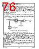
76 / 174 page  5.0 General-Purpose Input/Output (GPIO) Ports (Continued) 76 www.national.com Revision 1.1 Event Type and Polarity Two trigger types of event detection are supported: edge and level. An edge event may be detected on a source pin transi- tion either from high to low or low to high. A level event may be detected when the source pin is either at high or low level. The trigger type is determined by Event Type (bit 4 of GPCFG1 register). The direction of the transition (for edge) or the polarity of the active level (for level) is determined by Event Polarity (bit 5 of GPCFG1 register). Active edge refers to a change in a GPIO pin level that matches the Event Polarity bit (1 for rising edge and 0 for falling edge). Active level refers to the GPIO pin level that matches the Event Polarity bit (1 for high level and 0 for low level). The corresponding bit in GPEVST register is set by hardware whenever an active edge or an active level is detected regardless of the GPEVEN register setting. Writing 1 to the Status bit clears it to 0. Writing 0 is ignored. A GPIO pin is in event pending state if an active event has occurred (the corresponding bit in GPEVST register is set) and the corresponding bit in GPEVEN register is set. 5.3.2 System Notification System notification on GPIO-triggered events is achieved by asserting an interrupt request via the Interrupt Serializer in the LPC Bus Interface. The system notification for each GPIO pin is controlled by the corresponding bit in GPEVEN register together with bit 0 of GPEVR register. System notification by a GPIO pin is enabled if the corresponding bit of GPEVEN register is set to 1. The event routing mechanism is shown in Figure 12. Figure 12. GPIO Event Routing Mechanism for System Notification The system notification to the target is asserted if at least one GPIO pin is in event pending state. The selection of the target (for system notification) is determined by the GPEVR register. The specific IRQ number is deter- mined by the IRQ selection procedure of the device configuration. The assertion of IRQ (as a means of system notification) is disabled either when the GPIO functional block is deactivated or when VDD3 power is off. System notification through IRQ or SCI (see Section 6.2.4 on page 84) can be initiated by software by writing to the Data Out bit (in GPDO or GPDIO register) of a GPIO pin. This is possible only if the output of the corresponding GPIO pin is enabled, pin multiplexing is selected for the GPIO function (see Section 1.3 on page 15) and the GPIO event is routed to IRQ or SCI. System notification is asserted according to the actual level at the GPIO pin driven by the GPIO output and/or by external cir- cuitry. The level driven by the GPIO output should not cause a contention with the level driven by the external circuitry. A pending edge event may be cleared by clearing the corresponding GPEVST bit. However, a level event source may not be released by software (except for disabling the source) as long as the pin is at active level. When level event is used, it is also recommended to disable the input debouncer. Upon deactivation of the GPIO functional block and while VDD3 power is off, access through the LPC bus to the runtime registers (GPEVST and GPEVEN) is disabled. All means of system notification that include the target IRQ number are de- tached from the GPIO and de-asserted. When VDD3 power is off, the status bits of the GPIO pins connected to a VDD-powered device (VDDLOAD = 1) are cleared, however the status bits of the GPIO pins connected to a VSB-powered device (VDDLOAD = 0) are not affected. Before enabling any system notification, it is recommended to set the desired event configuration and then verify that the status registers are cleared. GPIO Event Pending Indication IRQ Event Routing Logic Enable IRQ Event Routing Register Bit 0 (GPEVR) Routed Events from other GPIO Pins Routing GPIO Pin GPIO Event to |
|
链接网址 |
| ALLDATASHEET是否为您带来帮助? [ DONATE ] |
关于 Alldatasheet | 广告服务 | 联系我们 | 隐私政策 | 数据表链接 | 链接交换 | 制造商名单 All Rights Reserved©Alldatasheet.com |
| Russian : Alldatasheetru.com | Korean : Alldatasheet.co.kr | Spanish : Alldatasheet.es | French : Alldatasheet.fr | Italian : Alldatasheetit.com Portuguese : Alldatasheetpt.com | Polish : Alldatasheet.pl | Vietnamese : Alldatasheet.vn Indian : Alldatasheet.in | Mexican : Alldatasheet.com.mx | British : Alldatasheet.co.uk | New Zealand : Alldatasheet.co.nz |
|
Family Site : ic2ic.com |
icmetro.com |
 Chinese ▼
 English
 Chinese
 German
 Japanese
 Russian
 Korean
 Spanish
 French
 Italian
 Portuguese
 Polish
 Vietnamese
 Indian
 Mexican
 British
 New Zealand